Original Article
, Volume: 14( 13)Quantum Confinement Effects on Absorption Spectrum Line Broadening of CdSe Artificial Atoms
- *Correspondence:
- Al Yamani K , Department of Physics, College of Science, Aleppo University, Aleppo, Syria, Tel: 963938386719; E-mail: alyamani.k@gmail.com
Received: July 11, 2016; Accepted: October 19, 2016; Published: November 20, 2016
Citation: Batal MA, Al Yamani K. Quantum Confinement Effects on Absorption Spectrum Line Broadening of CdSe Artificial Atoms.Mater Sci Ind J. 2016;14(13):105.
Abstract
Multi layers CdSe artificial atoms system was prepared using spin coating method. Using Williamson-Hall method, which is based on X-ray diffraction (XRD) broadening line profile, structural parameters of fluorine-doped-SnO2/CdSe (FTO/CdSe) system were calculated. The XRD spectrum reveals that CdSe nanoparticles have hexagonal structure, have high strain, show deposition layer, with more stress and strain (Crystallite size (6.16 Å), lattice constant C (7.16 Å), effective strain (0.7377) between the nano crystals and dislocation (irregular) [26.443 × 10²⁰ (lin.m-2)] were determined), which was later confirmed by analysis absorption spectrum broadening method. By performing fitting between experimental and theoretical absorption using Gaussian profile and Doppler broadening line, different electronic transitions were deduced and other broadening curve were studied such as effect of particle size on artificial atoms. With performing more accurate fitting, results reveal existence of two intensities lines attributed to diffusion layer between FTO and CdSe artificial atoms.
Keywords
CdSe; Artificial atoms; XRD broadening; Absorption spectra; Doppler broadening
Introduction
A quantum dot is a man-made solid-state structure which is able to confine one or several electrons and/or holes to a nanometer-scale potential minimum [1]. The size of a typical QD ranges from a few lattice constants to a few micrometers. Theory and modelling of the electronic structure and carrier dynamics of strain-induced quantum dot (SIQD) were discussed [2]. The lattice mismatch between the superficial CdSe stressor island and the FTO substrate induces a smooth and nearly parabolic strain deformation potential into the QW. As a result of the parabolic deformation potential, SIQD exhibit a uniquely regular and atomic-like photoluminescence spectrum. The weak potential barriers (shoulders) in the schematic band diagram of the SIQD result from the strain induced band-edge deformation. However, in a full 3D analysis including piezoelectricity these shoulders become superimposed with piezoelectric effects and partly disappear. QDs are frequently embedded in or grown on other materials with different elastic constants and lattice parameters. In such case, due to the lattice mismatch, the consequent elastic strain within the QDs is known to impact their electronic structure and hence opto-electronic properties [3]. Strain can shift the valence and conduction bands, change band gap, cause trapping of carriers and excitons, shift the oscillator strength of indirect band gap clusters [4], and in some piezoelectric materials (e.g. group III-V materials) even cause electrical fields [5]. Although the major effect is due to dilatational strain, axial and shear components can break the cubic symmetry (of most semiconductors) and lead to splitting of the light and heavy hole bands. In short, strain mediated control of electronic properties is an intensely researched subject of considerable technological importance in the context of both bulk systems and nanostructures. A wide range of approaches to assess the effect of mechanical strain on band structure is available, ranging from all-electron methods to approximate ab initio approaches like self-consistent density functional theory (DFT), empirical pseudopotential method (EPM), tight binding (TB), and envelope function method (EFM) [5].
A particularly useful feature of these materials is that the optical transitions broadened over a range comparable to the spacing between them, such that they strongly absorb light over a wide energy range. This feature, however, makes it difficult to study the origins of the broadening because individual transitions are difficult to discern. Previous work has characterized the transitions for ensembles of NCQDs of various radii.
To increase intensity of emission light and efficiency of PL spectra of transport hole or electrons layer insert between electrode and (P or N) semiconductor layer. In this paper, homogeneous and inhomogeneous broadening of optical absorption profile at room temperature of [FTO/TiO2(polystyrene)/CdSe(QDs)/PANI/EL] LEDs is investigated to show the influence of quantum confinement on absorption spectra. Using Williamson-Hall method, the effect of confinement on different layer structure is illustrated.
Materials and Methods
Microscopic slides, K2Cr2O7 for cleaning glass slides, HF (fluoric acid), SnCl2.2H2O, ethylene glycol, polyaniline (PANI), polyvinyl alcohol (PVA), CuCl2, KI, Se powder, Cd(CH3COO)2.4H2O, hydrazine, and deionized water were used.
Synthesis of FTO/TiO2 (polystyrene)/CdSe(artificial atoms)/EL/Ag
Preparation of transparent conducting fluorine-doped-tin oxide (FTO): Microscopic slides were cleaned using K2Cr2O7, and then were emerged in diluted fluoric acid (HF) for 10 minutes for scratch external surface of microscopic slides. After that microscopic slides were heated in electrical oven to 500°C. SnCl2.2H2O (5 g) dissolved in 20 ml of ethylene glycol and sprayed on microscopic slides several times each 5 min. The deposited resistance film SnO2 measured and it is 13 Ω to 14 Ω.
Preparation of TiO2 (polystyrene): TiO2 (polystyrene) colloidal solution was prepared by dissolving 0.1 M of TiO2 in 50 ml of ethanol and heated to 50°C [6].
Preparation of CdSe (artificial atoms): Artificial atoms of CdSe were prepared by chemical solutions method. Cadmium citrate (Cd (CH3COO)2 .4H2O) was used as the cadmium source and sodium selenosulfate (Na2SeSO3) was chosen as the selenium source. Cadmium citrate (22.8 g) was dissolved in 100 ml of deionized water called solution A. Sodium selenosulfate which was prepared by dissolving 12.6 g of Na2SO3 in 100 ml of deionized water, adding selenium powder (7.96 g) to previous solution refluxed at 70°C for 3 h, red wine colored solution will appear called solution B. Solution A (20 ml) was added to 5 ml of solution B, ethylene glycol (5 ml), hydrazine hydrate (5 ml) were added previously. CdSe colloidal solution was adjusted to pH 10 by adding 1 ml NaOH solution [7].
Preparation of electrolyte layer (EL): PVA powder (5 g) was dissolved in 100 ml of deionized water, stirred with magnetic stirrer at 70°C for 2 h. previous solution was aged for 1 h at room temperature called solution A. CuCl2.2H2O (5 g) was dissolved in 100 ml of deionized water at room temperature called solution B. KI (5 g) was dissolved in 100 ml of deionized water at room temperature called solution C. Solution B (10 ml) added to 30 ml solution A with continuous mixing for 1 h at room temperature. Then solution C added to previous solution 2 h later dropwise into the reaction vessel satisfying the ratio C=KI/CuCl2 (C=10), followed by stirring for another 2 h. The production process of CuI was according to the following reaction [8]:
Preparation of FTO/TiO2 (Polystyrene)/CdSe(artificial atoms)/EL/Ag: Using spin coating method for prepared FTO/TiO2 (polystyrene)/CdSe(artificial atoms)/EL/Ag as shown in Figure. 1.

Figure 1.a: Energy diagram of quantum well confinement of LED structure.

Figure 1.b: Box layer diagram of FTO/TiO2/MPA/CdSe/EL LEDs.
Results and Discussion
XRD spectrum of FTO/CdSe System
The X-ray diffraction (XRD) spectrum of FTO/CdSe film was recorded by Philips system using Cu Kα (λ=1.54056 Å) radiation with 2θ in the range 20º to 80º. Figure. 2 shows XRD spectrum, which reveals that CdSe sample, is polycrystalline in nature having all peaks corresponding to the specific planes. The extra peaks observed for CdSe artificial atoms at 2θ (degree) 2θ=29.18°, 41.75°, 48.75° with maximum intensity peak which corresponding oriented planes (101), (102), (112) respectively, and for 2θ equal 2θ=25°, 35°, 37°, 52°, 62.1°, 65.8° are different angles for FTO corresponding to (110), (101), (200), (221), (310), (301) respectively.
The lattice spacing, d, calculated from the Bragg’s formula [9]:
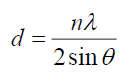
For first peak, d=3.06 Å, n=1, 2θ =29.18° for CdSe artificial atoms. For FTO, d=3.56 Å at n=1, 2θ=25°
The peak broadening in XRD patterns may arise from several reasons such as smaller crystallite size, instrumental error and strain broadening: βtot=βv+βs+βm. As in the present case, proper precautions have been considered during scanning such as slow scan rate. Therefore, the observed broadening (Figure 2) is due to the strain and smaller crystallite size, where their contribution to peak broadening is independent of each other. Therefore, total broadening can be written as sum of these two as βtotal= βstrain + βcrystallite size by neglected broadening instrument, using Williamson-Hall equation [10]:
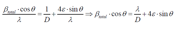

Figure 2: XRD spectrum of FTO/CdSe.
Where ε is the effective strain present in the material, d the effective crystallite size, λ the wavelength of X-ray radiation, β is the full width at half maximum (FWHM) and θ the diffraction angle. By plotting βtotal. cos θ in function of sin θ, negative slope of pure CdSe artificial atoms as shown in Figure 3 indicate the presence of effective compressive strain in the crystal lattiec. Effective strain for CdSe artificial atoms ε1=0.7377.

Figure 3: (a) Williamson-Hall plot for FTO (b) Williamson-Hall plot for CdSe (artificial atoms).
For FTO, ε1=0.00615. In materials science, a dislocation is a crystallographic defect, or irregularity, within a crystal structure. The presence of dislocations strongly influences many of the properties of materials. The dislocation density δ has been calculated by using the formula [11]:
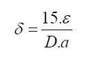
Where ε is effective strain value, D the crystallite size, a hexagonal lattice constant for CdSe artificial atoms equal 4.29 Å. The lattice constant C is determined for hexagonal structure by the following expression [9]:
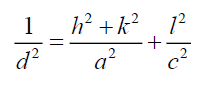
Where h, k and l represent lattice planes (202) which corresponding with diffraction angle 2θ=56.8°. Lattice constant C is close to standard value 7.01 Å. Table 1 shows the different parameters calculated using Williamson-Hall for both CdSe artificial atoms and FTO layer. It reveals the high strain parameter of FTO and CdSe due to quantum confinement of one CdSe layer quantum confinement of CdSe artificial atoms. The depth and size of the QD carrier confinement can be tuned by changing the widths and material composition of the well and barrier layers. A phenomenological view of the electronic and optical properties of SIQD can be obtained using a simple two-band effective-mass model. A more realistic description, based on fully 3D multiband envelope wave function approximation (EFA).
| δ (lin.m-2) Dislocation density | ε Effective strain | d (Å) Lattice spacing | D (Å)Average crystallite size | C (Å) Lattice constant | |
|---|---|---|---|---|---|
| CdSe (artificial atoms) |
26.443 × 10² | 0.7377 | 3.06 | 6.16 | 7.16 |
| FTO | 29.65 × 10¹⁸ | 0.00615 | 3.56 | 6.26 | 5.47 |
Table 1: Summary of XRD Spectrum.
The total QD confinement of electrons and holes is the sum of the QW carrier confinement  (vertical confinement) and the strain-induced carrier confinement
  (lateral confinement) [12]. Figure 4 shows schematically how the strain-induced confinement potential is created in the conduction band (a) and valence band (b) of the QW. The compressive strain, caused by the lattice mismatch between the substrate and the CdSe (MPA) QDs. QW gives rise to a uniform raising of the QW conduction and heavy-hole band-edges. The strain also gives rise to a significant splitting of the heavy and light hole bands. It is concluded that the strain greatly prefers the confinement of heavy holes to the QW. The confinement of light holes is much weaker.

Figure 4: Schematic illustration of the strain-induced band-edge deformation for (a) the conduction and (b) the valence bands.
For FTO, the lattice constant C is determined for hexagonal structure by the following expression [13]:
Where h, k and l represent lattice planes (101) which is corresponding with diffraction angle 2θ=37.52°, a=4.73 Å for hexagonal lattice of FTO.
Absorption spectra of FTO/TiO2(Polystyrene)/MPA/CdSe(artificial atoms)/EL LED
To know different process of broadening line in the matrix FTO/CdSe and to reveal these different broadening types absorption spectra of FTO/TiO2(Polystyrene)/MPA/CdSe(artificial atoms)/EL LED carried out using spectrophotometer (UV Win5 V5.2.0). Absorption spectrum in Figure 5 reveals two peaks centered at wavelength 375 nm and 596 nm.

Figure 5: Absorption spectra of FTO/TiO2(Polystyrene)/MPA/CdSe QDs/EL.
The broad absorption spectrum at 596 nm related to electronic transitions in CdSe artificial atoms the highest occupied molecular orbital (HOMO) originates from Se 4p atomic orbitals, and the lowest unoccupied molecular orbital (LUMO) from Cd 5s atomic orbitals. Those electronic states are strongly dependent on the size (the degree of confinement). Because increasing the aspect ratio only reduces confinement along the c-direction, some energy levels are sensitive to the length of the NR much more than others, and level crossing occurs. For HOMO levels, the levels consisting of a Se 4p component are more dependent on the length, by increasing the nano rods length; the energy levels converge into several energy levels. This is a transition from zero-dimension confinement (0D) to one dimensional (1D), where a continuous band forms along the c-axis. For this reason, more versatile nano electronic and optical devices, which combine the advantage of 0D and 1D confinement, can potentially be made using quantum NRs as building blocks [9], where the absorption peak at 375 nm due to direct transition for TiO2. From Figure 4 the high absorption peak at wavelength 300 nm related to FTO band-to-band transition is observed. Result of homogeneous broadening in absorption spectra was caused for several reasons; quantum confinement and multi high barriers in stature of FTO/TiO2/CdSe/EL system and different sizes of artificial atoms of CdSe.
Homogenous broadening in electronic transitions in CdSe artificial atoms LEDs
To ensure electronic transitions in CdSe artificial atoms which is found in structure of FTO/TiO2/CdSe/EL system, theoretical energy of electronic transitions as in Figure 6. By using Gaussian profile, for all theoretical energies transitions of CdSe artificial atoms [14,15], energy band gap of FTO and energy transition of TiO2 with using experimental values from absorption spectra. When Doppler broadening is dominating, velocity distribution is dominating on line spectra. In this case, experimental line spectral given by distribution of velocity for atoms or molecular as shown [14]:
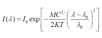

Figure 6: (a) Theoretical electronic transition in CdSe artificial atoms and (b) Experimental absorption spectra of CdSe Nano crystal (R=4.1 nm) these energies [15].
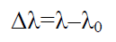
Where I(λ) is line spectra module (maximum intensities of line spectral).
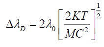
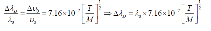
Where T is absolute temperature (300 K). Table 2 shows values of broadening in absorption wavelength peak.
| γ0(nm) | E(eV) | Transition | ΔγD(nm) |
|---|---|---|---|
| 280 | 4.4 | FTO | 0.0080 |
| 373 | 3.33 | TiO2 | 0.0106 |
| 521 | 2.38 | CdSe 1S(e) → 3S1/2(h) | 0.0146 |
| 568 | 2.18 | CdSe 1P(e) → 1P1/2(h) | 0.0161 |
| 620 | 2 | CdSe 1S(e) → 2S3/2(h) | 0.017 |
| 642 | 1.93 | CdSe 1S(e) → 2S3/2(h) | 0.018 |
Table 2: Absorption wavelength, their energy, electronic transitions and value of broadening in absorption wavelength peak.
Figure 7 shows theoretical transitions (in different colors), experimental absorption spectra. From Figure 7, it is identified between experimental and theoretical transitions for all layers of LED structure. By taking Gaussian broadening for theoretical transitions for all layers of LED and compare with experimental absorption spectra by using Mathcad program. To do fitting between experimental and theoretical absorption spectra: first, different spectral lines were traced using theoretical energy transitions for FTO and CdSe artificial atoms as it indicated in Table 1 and Figure 7 and using Gaussian shape which use Doppler broadening.

Figure 7: Theoretical transitions (in different colors) and experimental absorption spectra (black line).
Secondly, convolution was made for these traced lines and doing a rough fit with theoretical one. Figure 7 shows the fitting between experimental and calculation absorption spectra as it clears the fitting was very well but not 100%.Figure 8 shows the 100% fitting between experimental and theoretical absorption spectra. It reveals two absorption peaks located at 365 nm. These small peaks refer to absorption from diffused layer between FTO and CdSe layer.

Figure 8: Fitting experimental absorption spectra with theoretical electronic transitions.
Also, it should be noted that shift in energy transition results from distribution of different size of cluster atoms broadening, confinement broadening and Doppler broadening.
Ratio of broadening, which due to size distribution and Doppler can be neglected by comparing with quantum confinement broadening.
Conclusion
FTO/TiO2(polystyrene)/CdSe/EL system was prepared using spin coated method. Quantum confinement effect on these structures was studied through XRD spectra using Williamson-Hall Method which produces crystallite size distribution. This more accurately separates the instrumental and sample broadening effects. It also gives average length size rather than average volume size. Broadening in absorption spectra lines reveal new electronic transitions due to diffusion layer between CdSe artificial atoms and TiO2 layers is shown in Table 3. There was energy shift between theoretical energy transitions and experimental absorption lines in CdSe artificial atom due to different effects such as quantum confinement between layers of system, different size of cluster in one layer and diffusion between layers particularly between CdSe artificial atoms and TiO2 layers.
| Theoretical energy transitions (eV) | Broadening energy transitions (eV) | Energy shift (eV) |
|---|---|---|
| 1.74 CdSe 4P(h) → 5S1/2(e) | 1.44 CdSe 4P(h) → 5S1/2(e) | 0.30 |
| 1.93 CdSe 1S(e) → 1S3/2(h) | 3.26 CdSe 1S(e) → 1S3/2(h) | 1.33 |
| 2 CdSe 1S(e) → 2S3/2(h) | 1.95 CdSe 1S(e) → 2S3/2(h) | 0.049 |
| 2.183 CdSe 1P(e) → 1P3/2(h) | 2.37 CdSe 1P(e) → 1P1/2(h) | 0.196 |
| 2.380 CdSe 1S(e) → 3S1/2(h) | 3.30 CdSe 1S(e) → 3S1/2(h) | 0.929 |
| 3.306 VB → CB TiO2 | 3.40 VB → CB TiO2 | 0.096 |
| 4.428 VB → CB FTO | 5.10 VB → CB FTO | 0.673 |
Table 3: Theoretical electronic transitions, broadening energy transitions and difference between it in (eV).
References
- Ashoori RC. Electrons in arti?cial atoms.Nature.1996;379(6564):413-19.
- Lipsanen H, Sopanen M, Ahopelto J.Luminescence from excited states in strain-induced inas quantum dots.PhysRev B.1995;51(91):13868-871.
- Davies JH.The physics of low-dimensional semiconductors: An introduction. Cambridge: Cambridge University Press; 1998.
- Singh J.Physics of semiconductors and their heterostructures. New York: McGraw-Hill; 1992.
- Boxberg F,Tulkki J.Theory of the electronic structure and carrier dynamics of strain-induced (Ga,In) as quantum dots.Rep Prog Phys. 2007;70(8):1425-71.
- Nguyen V. Cadmium selenium quantum dot photodiodes. National Nanotechnology Infrastructure Network.2007;34-5.
- Batal MA, Al-yamani K. Optical properties ofcolloidal CdSe/CdS/Zns/PVPQDs core/shellsembedded in fatty acid medium.Nano Tech Nano Sci Ind J.2015;9(1):19-21.
- Sheha E, Khoder H, Shanap TS, et al. Structure, dielectric and optical properties of p-type (PVA/CuI) nanocomposite polymer Electrolyte for photovoltaic cells. Optik. 2012;123(13):1161-66.
- Suthan Kissinger NJ, Jayachandran M, Perumal K, et al. Structural and optical properties of electron beam evaporated CdSe thin films. Bull Mater Sci. 2007;30(6):547-51.
- Prabhu Y, Rao K, Kumar V, et al. X-ray analysis by Williamson-Hall and size-strain plot methods of ZnO nanoparticles with fuel variation. World Journal of Nano Science and Engineering. 2014;4(1):21-8.
- WangLW, Zunger A. High-energy excitonic transitions in CdSe quantum dots.J Phys Chem B. 1998;102 (34):6449-54.
- Ahopelto J, Sopanen M, Lipsanen H. Tailoring of energy levels in strain-induced quantum dots. Japan J Appl Phys. 1999;38(Pt 1, Number 2B):1081-4.
- Ayeshamariam A. Synthesis, structural and optical characterizations of Sno2 nanoparticles.Journal on Photonics and Spintronics. 2013;2(2):4-8.
- Martin WC, Wiese WL. Atomic Spectroscopy - A compendium of basic ideas, notation, data, and formulas. National Institute of Standards and Technology, Gaithersburg, Maryland, USA; 2009.
- Horodyska P, Nemec P, Sprinzl D, et al. Exciton spin dynamics in spherical CdS quantum dots. Phys Rev B. 2010;81:045301.