Original Article
, Volume: 13( 1)Growth and Characterization of CdS Nanoparticles for Phtotovolatic Cell Application
- *Correspondence:
- Jamil Yaseen, Department of Physics, Dr. Babasaheb Ambedkar Marathwada University, Aurangabad, India, Tel: 02402400431; E-mail: jamilyaseen8@gmail.com
Received: January 12, 2018; Accepted: February 07, 2018; Published: February 12, 2018
Citation: Yaseen J, Sable PB, Dharne GM. Growth and Characterization of CdS Nanoparticles for Phtotovolatic Cell Application. Phys Chem Ind J. 2018;13(1):120.
Abstract
Nano-crystalline semiconductor materials have attracted considerable attention due to their particle size dependent physical properties and very large specific surface area which are not present in bulk materials. Usually they are synthesized with organic ligands to disperse them from agglomeration. However, these ligands can act as series resistance in the active layer of solar cells. In this work cadmium sulfide (CdS) precipitates were prepared from cadmium and sulfide ion solutions without any ligands at different solution temperature and synthesis time. The obtained CdS precipitates were washed by rinsing with methanol and by centrifugation with water and methanol. By using Fourier transform infrared spectroscopy (FTIR) impurities were observed on the surface of rinsed CdS samples and they had been eliminated after washing by centrifugation (not shown here). X-ray diffraction (XRD) patterns indicate that the obtained products were of hexagonal structure. The average size of the CdS crystallites found by Scherrer formula 12 nm before centrifugal washing and 6 nm after washing. The best cell prepared with CdS nanoparticles showed a photocurrent (Jsc) of 2.2 mA/cm2 and a photovoltage (Voc) of 0.84 V, measured in air at room temperature under 100 mW/cm2 illumination in a solar simulator.
Keywords
Cadmium acetate; Methanol; CdS; Nanoparticles; XRD
Introduction
Solar energy conversion is a highly attractive process for clean and renewable power for the future. Solar Energy is an only way to rise out of global poverty. We always intend to make our lives comfortable, energizing and productive. Mankind is using energy in many ways to improve living standard. We depend on energy for almost everything in our life. Due to the enormous amount of energy consumption, the world is facing an energy crisis. We have very limited sources of energy like coal, petroleum and natural gases. Now-a-days, most of the energy is produced by fossil fuel and coal. Coal is the main source of carbon dioxide emissions in the world resulting global warming. From environmental point of view, a burning of fossil fuel depletes our non-renewable energy source and produce pollution. More combustion of fossil fuel can deplete the non-renewable energy sources. In nature, cost effective and pollution free. Solar energy is abundant and easily available, renewable energy source in world, especially in India.
However, we need to use it more economically. Solar cell is also called as photovoltaic cell, which converts solar energy into electrical energy. Today, silicon based solar cells are commercially produced because of the abundant supply of silicon row material and its comparatively high efficiency. However, very pure Silicon is needed hence the price is very high compared to the power output [1].
For nanometer proportioned systems, their optical and electronic properties become size-dependent. Thus, chemical control over the growth and size of particles should allow a corresponding control over these properties [2]. In particular, considerable interest has centered on the synthesis of nanometer-size semiconductor particles [3,4]. The unique electronic and optical properties of semiconductor nanomaterials constitute the fundamental reason behind their technological importance. Cadmium sulfide (CdS) is one of the most important II–VI group semiconductors. It has been proved to be an excellent photoactive and charge transport material in optoelectronic devices [4], and its direct band-gap of 2.4 eV is appropriate to be an acceptor in hybrid photovoltaic (HPV) devices [5-7]. CdS nanoparticles exhibit structural, optical and photo-conducting properties that are very different from their bulk properties that make them attractive for their possible application in solar cell, photo detector, laser, LED etc. [4]. Nanoparticles of CdS are usually synthesized in presence of ligands. These are lineal organic compounds that one of their two (head or tail) terminals is attached onto the surface of the nanoparticles and the other is solvated by the solvent molecules. In this way the nanoparticles were surrounded by these organic molecules and are separated one from each other under the electrostatic repulsion between the free terminals of the ligands. However, for solar cell applications, these ligands are obstacles to charge carrier transport, leading to a low photocurrent. The removal of the ligands in nanoparticles requires another chemical process [8-12].
Experimental Procedure
0.1 M solution of Na2S and 0.1 M solution of cadmium acetate [Cd(OOCCH3)2·2H2O] were prepared in methanol. The temperature reaction was chosen as 0°C or 25°C (room temperature). The cadmium ion solution was added slowly into the sulfide one and the resulting solution turned from transparent to yellow color, which is indicative of the immediate formation of CdS product. The reaction time was stopped at 0.5 h and 24 h at each temperature. The obtained CdS precipitates were washed in two ways: (a) rinsed by about 50 mL of methanol (called rinsed samples), and (b) washed by centrifugation for 10 times with 50 mL of deionized water each time and the last one with 50 mL of methanol (called washed sample). All the final products were dried at room temperature for 48 h.
Characterization
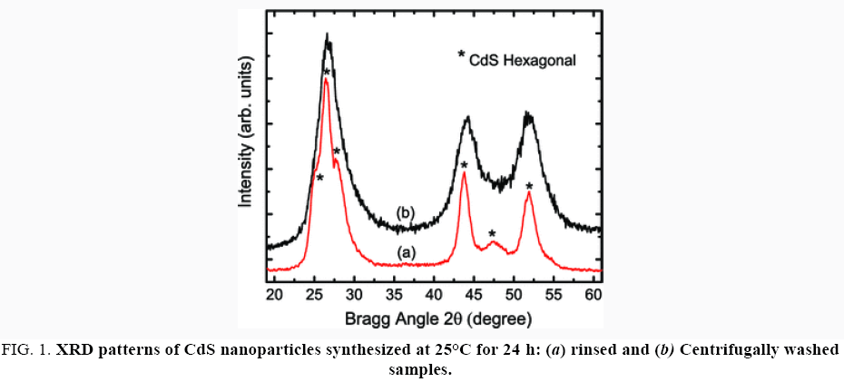
X-ray diffraction (XRD) patterns were recorded in a BRUKER D8 Advance (CuKα-radiation λ=0.154 nm), with a scanning rate of 1°/min from 10° to 70° in 2θ range (Figure 1).
Figure 1: XRD patterns of CdS nanoparticles synthesized at 25°C for 24 h: (a) rinsed and (b) Centrifugally washed samples.
The average crystallite sizes of CdS nanoparticles were estimated by Scherrer equation:
 (1)
(1)
where D is the crystalline grain size, K is a Scherrer constant (shape factor) taken to be 0.94, λ is the wavelength of the Xray radiation, β is the full width at half maximum (FWHM) of the diffraction peak, and θ is the angle of diffraction at that peak.
It was found that the average crystallite size was about 12 nm for rinsed and 6 nm for washed samples. Although the discrepancy existed in size numbers provided by the two experimental methods, it is evident that the centrifugal washing process reduced the crystallite size in CdS nanoparticles from 6 nm to 12 nm down to 3 nm–5 nm. The product yield was also estimated for different reaction temperature and time by adding 50 mL of 0.1 M Cd(OOCCH3)2·2H2O into 50 mL of 0.1 M Na2S solution. It seems that 30 min of reaction was enough to obtain more than 90% of the final CdS product.
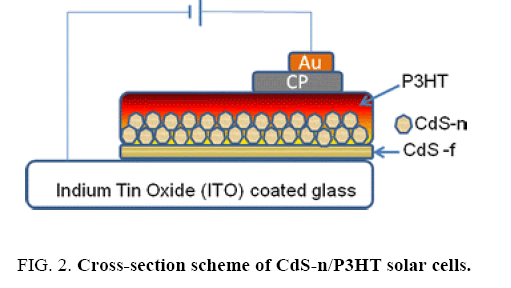
The build of the solar cells consisted in the following steps: 50 nm of CdS thin film was deposited on transparent conductive glass substrate (indium–tin–oxide coated glass slides with sheet resistance of 15 Ω per square, Lumtec) by chemical bath deposition [13] described as CdS-f in the hybrid structure. Subsequently, CdS nanoparticles were deposited on the CdS thin film by spin-coating. P3HT was synthesized by a chemical oxidation method [14]. P3HT solution was prepared by dissolving the polymer product in 1,4-dichlorobenzene and dripped on top of the CdS nanoparticle layer. The P3HT film was formed after a fast-drying process (70°C–80°C). Carbon paint (CP) was spread on the polymer surface and dried in air. Then gold contacts of about 40 nm thickness were deposited by evaporation on top of CP. The use of CP was to improve the ohmic contact and avoid the gold atoms diffusion. The structure of the cells was: ITO/CdS-f/CdSn/ P3HT/CP/Au. Figure 2 illustrates the cross-section scheme of those CdS/P3HT solar cells. Except for metal contact, all the cell preparation process was carried out in air. The whole device was annealed in air at 120°C for 30 min. Current–voltage (I–V) curves of solar cells was taken under illumination of one Sun with a solar simulator (Oriel) and the intensity of the Xenon lamp was adjusted to 100 mW/cm2. The electrical characterizations of hybrid solar cells were carried out in air under ambient conditions.
Results and Discussion
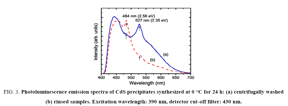
The centrifugal washed CdS powder was finer than the rinsed one, that is, the centrifugation process could break down CdS clusters into smaller ones. An indirect measurement of particle size is the BET method, which consists in determining the specific surface area of powder samples by physical absorption of an inert gas (N2, for example). The larger the specific area, the smaller the average particle size [4]. The BET surface area of rinsed CdS nanoparticles was of 66.55 m2/g, and for centrifugal washed samples that number was almost doubled: 127 m2/g, which is consistent with the physical appearance of the two types of CdS powders, it is valid to assume that the washed CdS precipitates still kept the hexagonal structure but with smaller crystallites inside the particles (Figure 3).
Figure 3: Photoluminescence emission spectra of CdS precipitates synthesized at 0 °C for 24 h: (a) centrifugally washed (b) rinsed samples. Excitation wavelength: 390 nm, detector cut-off filter: 430 nm.
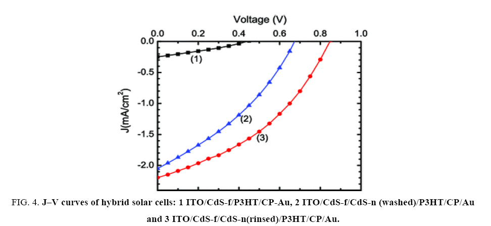
Finally, the use of CdS nanoparticles in hybrid solar cells was experimented. The use of a solution deposited CdS thin film (CdS-f) on ITO surface served as a sealing layer to prevent short-circuit between ITO and the metal contact. Then CdS nanoparticles were deposited as a rough layer CdS-n, which allowed a posterior good permeation of P3HT macromolecules into the inorganic layer and enlarged the CdS-n/P3HT interface. Being the same semiconductor compound, the heterojunction of CdS thin film and P3HT (ITO/CdS-f/P3HT/CP-Au) also generated photovoltage (Voc) and photocurrent (Jsc), as evidenced in Figure 4, although with inferior photovoltaic performance. The use of CdS nanoparticles (CdS-n) between CdS-f and P3HT improves largely those parameters; Figure 4,shows the J–V curves of the best CdS/P3HT hybrid cells with washed CdS nanoparticles (ITO/CdS-f/CdS-n-washed/P3HT/CP/Au) and rinsed CdS ones (ITO/CdS-f/CdS-n-rinsed/P3HT/CP/Au) where the CdS powders were synthesized at 25°C for 24 h and the cells were fabricated under the same procedure.
Figure 4: J–V curves of hybrid solar cells: 1 ITO/CdS-f/P3HT/CP-Au, 2 ITO/CdS-f/CdS-n (washed)/P3HT/CP/Au and 3 ITO/CdS-f/CdS-n(rinsed)/P3HT/CP/Au.
Photovoltaic parameters of the J-V curves shown in Figure 4 are listed in Table 1, and the maximum power conversion efficiency was about 0.72%.
| Structure (CdS at 0°C for 24 hr) | Jsc(mA/cm2) | Voc(V) | FF | η(%) |
|---|---|---|---|---|
| (1) ITO/CdS-f/P3HT/CP-Au | 0.24 | 0.43 | 0.3 | 0.03 |
| (2) ITO/CdS-f/CdS-N-washed P3HT/CP-Au | 2.05 | 0.67 | 0.34 | 0.47 |
| (3) ITO/CdS-f/CdS-n rinsed/P3HT/CP- Au | 2.19 | 0.84 | 0.39 | 0.72 |
Table 1: Photovoltaic parameters of the J-V curves.
It is seen that the two cells with CdS nanoparticles (rinsed and washed) gave a good Jsc (current density at voltage equal to zero) above 2 mA/cm2. However, the rinsed CdS nanoparticles gave a higher Voc (voltage at current equal to zero) than the washed ones. This phenomenon can be explained by the fact that a higher density of the surface states in washed CdS samples should lead to a higher probability of charge recombination at CdS-n/P3HT interface, which in turn should reduce the Voc of the heterojunction [15]. On the other hand, the CdS crystallite size should also play an important role in the photovoltaic behavior of the cells, which could not be clearly observed because of the surface states in washed CdS samples. In literature, similar CdS/P3HT heterojunctions have been reported and the obtained power conversion efficiency varied from 0.06% [7] to 4.1% as CdS is grafted in the highly ordered P3HT nanowires [16]. Further research effort should be addressed to improve the photovoltaic performance of hybrid solar cells.
Conclusion
Nanoparticles of cadmium sulfide were synthesized from cadmium and sulfide ion solution in methanol without any ligands or dispersants. The reaction temperature was chosen at 0°C or 25°C and the reaction time, for 0.5 h or 24 h. Both types of samples showed a crystalline hexagonal structure, although the centrifugal washing reduced the crystallite size from 12 nm to 6 nm. Photoluminescence spectra also suggest the presence of impurities at the surface of rinsed samples. The photocurrent density of hybrid solar cells with CdS nanoparticles and poly(3-hexylthiophene) was higher than 2 mA/cm2, and the photovoltage of the same cells reached to 0.84 eV, which will be lowered down to 0.67eV if the CdS nanoparticles were smaller.
Acknowledgement
One of the authors (Jamil Yaseen & G. M. Dharne) are grateful to Professor and Head R. P. Sharma for providing XRD and UV-VIS spectroscopy facility at Department of Physics Dr. BAMU Aurangabad.
References
- Selene Coria-Monroy C, Arenas MC, Nicho ME, et al. Solution synthesized CdS nanoparticles for hybrid solar cell applications. J Mater Sci: Mater Electron.2014;26(8): 5539-45.
- Kotkata MF, Masoud AE, Mohamed MB, et al. Synthesis and structural characterization of CdS nanoparticles. Phys E. 2009;41(8):1457-65.
- Bhattacharya R, Das TK, Saha S. Synthesis and characterization of CdS nanoparticles. J Mater Sci: Mater Electron. 2011;22(12):1761-5.
- Elashmawi IS, Abdelghany AM, Hakeem NA. Quantum confinement effect of CdS nanoparticles dispersed within PVP/PVA nanocomposites. J Mater Sci: Mater Electron. 2013;24(8):2956-61.
- Jiang X, Chen F, Xu H, et al. Template-free synthesis of vertically aligned CdSnanorods and its application in hybrid solar cells. Sol Energy Mater Sol Cells. 2010;94(2)338-44.
- Alivisatos AP. Perspectives on the physical chemistry of semiconductor nanocrystals. J Phys Chem. 1996;100(31):13226-39.
- Zhong M, Yang D, Zhang J, et al. Improving the performance of CdS/P3HT hybrid inverted solar cells by interfacial modification. Sol Energy Mater Sol Cells. 2012;96:160-5.
- Al-Hussam MA, Abdul-Jabbar SJ. Synthesis, structure, and optical properties of CdS thin films nanoparticles prepared by chemical bath technique. J Assoc Arab Univ Basic Appl Sci. 2012;11(1):27-31.
- Jang J, Choi SH, Cho S, et al. Light-induced cleaning of CdS and ZnSnanoparticles: Superiority to annealing as a post-synthetic treatment of functional nanoparticles. J PhysChem C. 2012;116(29):15427-31.
- Moulé AJ, Chang L, Thambidurai C, et al. Hybrid solar cells: Basic principles and the role of ligands. J Mater Chem. 2012;22(6):2351-68.
- Zhou Y, Riehle FS, Yuan Y, et al. Improved efficiency of hybrid solar cells based on non-ligand-exchanged CdSe quantum dots and poly(3-hexylthiophene). ApplPhysLett. 2010;96(1):013304.
- Lokteva I, Radychev N, Witt F, et al. Surface Treatment of CdSe Nanoparticles for Application in Hybrid Solar Cells: The Effect of Multiple Ligand Exchange with Pyridine. J PhysChem C. 2010;114(29):12784-91.
- Robel I, Kuno M, Kamat P. Size-dependent electron injection from excited CdSequantum dots into TiO2nanoparticles. J Am Chem Soc. 2007;129(14):4136-7.
- Skompska M. Hybrid conjugated polymer/semiconductor photovoltaic cells. Synth Met. 2010;160(1,2):1-15.
- Cortina H, Pineda E, Campos J, et al. Photogenerated charge carrier recombination processes in CdS/P3OT solar cells: effect of structural and optoelectronic properties of CdS films. EurPhys J Appl Phys. 2011;55(3):30901.
- Ren S, Chang L, Lim S, et al. Inorganic–organic hybrid solar cell: Bridging quantum dots to conjugated polymer nanowires. Nano Lett. 2011;11(9):3998-4002.
