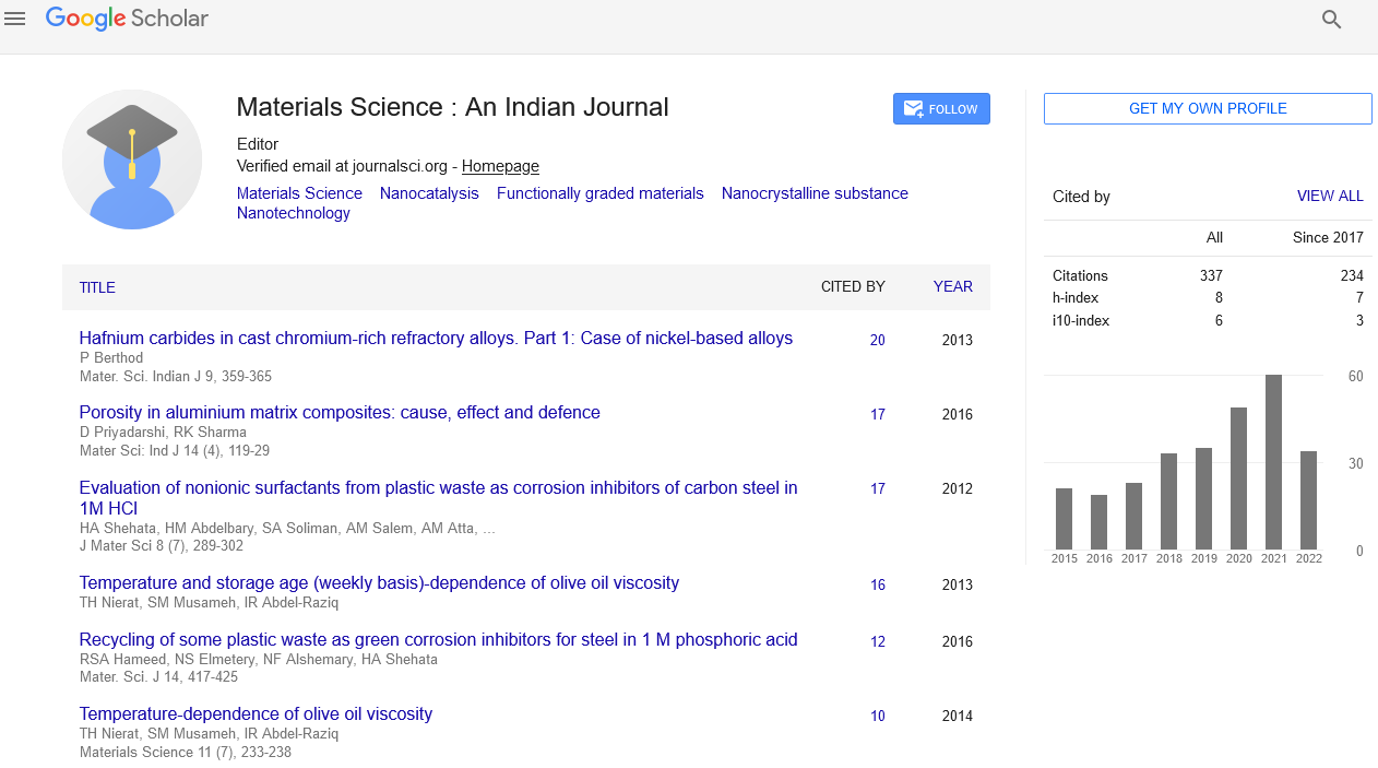
Editorial
, Volume: 23( 3)Atomic Force Microscopy and Nanoscale Surface Characterization
Isabelle Fournier* Department of Nanoscience and Materials Engineering, Grenoble Alpes University, France, *Corresponding author: Isabelle Fournier, Department of Nanoscience and Materials Engineering, Grenoble Alpes University, France, E-mail: ifournier.afm@nanomaterials.fr Received: Feb 04, 2025; Accepted: Feb 18, 2025; Published: Feb 27, 2025
Abstract
Abstract Atomic Force Microscopy (AFM) is a high-resolution scanning probe technique used to analyze surface topography and properties at the nanometer scale. Unlike electron-based imaging methods, AFM uses a sharp mechanical probe to scan surfaces and measure forces between the probe and the sample. This technique provides detailed information about morphology, mechanical properties, and surface interactions. This article discusses the principles, operational modes, and applications of atomic force microscopy in materials science. forces, Materials characterization Keywords: Atomic Force Microscopy, Nanoscale imaging, Surface topography, Scanning probe microscopy, Nanomechanics, Surface Introduction Atomic Force Microscopy is built on an elegant idea: instead of using light or electrons to see a surface, physically feel it with an extremely sharp probe. The probe, mounted on a flexible cantilever, scans across the sample surface while a laser detects tiny deflections of the cantilever caused by atomic-scale forces. These deflections are converted into high-resolution images that map the surface topography with remarkable precision.The interaction between the probe tip and the sample surface involves forces such as van der Waals forces, electrostatic forces, and mechanical contact forces. By monitoring these interactions, AFM can produce three-dimensional surface profiles at nanometer resolution. This makes it particularly useful for studying thin films, nanostructures, polymers, and biological materials [1].AFM operates in several modes, including contact mode, tapping mode, and non-contact mode. In contact mode, the tip remains in constant contact with the surface, which is suitable for hard materials. Tapping mode reduces lateral forces by intermittently contacting the surface, making it ideal for softer or delicate samples. Non-contact mode measures attractive forces without direct contact, minimizing potential damage [2]. Beyond imaging, AFM can measure mechanical properties such as stiffness, adhesion, and Citation: Isabelle Fournier. Atomic Force Microscopy and Nanoscale Surface Characterization. Macromol Ind J. 23(3):168. 1 © 2025 Trade Science Inc. www.tsijournals.com | Feb -2025 elastic modulus at very small scales. Force–distance curves obtained during tip interaction provide quantitative information about local mechanical behavior. This capability is particularly valuable in studying nanocomposites, coatings, and biological membranes [3].AFM can also be combined with other techniques to enhance functionality. Conductive AFM allows mapping of electrical properties, while magnetic force microscopy enables imaging of magnetic domains. Such variations expand the technique’s usefulness across fields including semiconductor research, magnetic materials analysis, and nanotechnology development [4]. Sample preparation for AFM is relatively simple compared to electron microscopy because ultrathin samples are not required. However, surface cleanliness and stability are important for obtaining accurate measurements. Recent advances have improved tip design and environmental control, allowing AFM to operate in liquids or controlled atmospheres [5]. Conclusion Atomic Force Microscopy is a versatile and powerful technique for exploring material surfaces at the nanoscale. By physically sensing atomic-scale interactions, AFM provides detailed topographical and mechanical information that is essential for nanomaterials research and surface engineering. It is a method that turns the act of “seeing” into a refined form of touch—where a tiny probe traces the landscape of matter and reveals hills and valleys measured in billionths of a meter. REFERENCES 1. Panwar AS, Singh A, Sehgal S. Material characterization techniques in engineering applications: A review. Materials Today: Proceedings. 2020 Jan 1;28:1932-7. 2. Panwar AS, Singh A, Sehgal S. Material characterization techniques in engineering applications: A review. Materials Today: Proceedings. 2020 Jan 1;28:1932-7. 3. Patel R, Chaudhary ML, Martins AF, Gupta RK. Mastering material insights: advanced characterization techniques. Industrial & Engineering Chemistry Research. 2025 Apr 25;64(18):8987-9023. 4. Sharma SK, Verma DS, Khan LU, Kumar S, Khan SB, editors. Handbook of materials characterization. New York, NY, USA Springer International Publishing; 2018. 5. Kassem H, Vigneras V, Lunet G. Characterization techniques for materials’ properties measurement. InMicrowave and Millimeter Wave Technologies From Photonic Bandgap Devices to Antenna and Applications 2010 Mar 1. Intech Open.