Short commentary
, Volume: 14( 13)Thin Film Solar Cells with Plasmonic Nanostructures
- *Correspondence:
- Gurjit Singh , Department of Physics, Sant Longowal Institute of Engineering and Technology Longowal, Sangrur 148 106, India, Tel: + 91-9501327600; E-mail: higurjit@yahoo.co.in
Received: July 28, 2016; Accepted: October 14, 2016; Published: October 20, 2016
Citation: Singh G, Verma SS. Thin Film Solar Cells with Plasmonic Nanostructures. Mater Sci Ind J. 2016;14(13):104.
Abstract
The solar cell industry is growing day by day due to rising prices of fossil fuels, the problem of global climate change and increasing demands of clean, efficient and low cost renewable energy. But the manufacturing cost of solar cells is an important aspect. However, thin film solar cells decreased the cost of the cell by reducing the thickness but trapping of enough light becomes crucial in these cells. By incorporating plasmonic nanostructures of different materials, configurations and geometries in thin film solar cell design, researchers measured an enhanced photocurrent attributed to the increased trapping of light scattered into a thin-film solar cell by metal nanoparticles excited at their surface Plasmon resonance and overall efficiency enhancement of about 8% have been achieved. Now, we are looking to design plasmonic solar cells with more efficiency in the photovoltaic industry.
Keywords
Photovoltaic; Plasmonics; Photocurrent; Surface plasmon resonance
Introduction
The photovoltaics is considered as a clean energy source compared to fossil fuels. A solar cell (SC) is a solid state electrical device which converts the energy of sunlight into electricity by the photovoltaic effect [1,2]. The basic principle of solar cell is that the incoming photons or sunlight must have the right energy, called the band gap energy (for Si ~ 1.11 eV, GaAs ~ 1.43 eV and CdTe ~ 1.49 eV), to knock out an electron. If the photon has less energy than the band gap energy, then it will pass through the material and if energy is more than the band gap energy then it is absorbed by the material. When photon is absorbed, its energy is given to the electron which excites the electron from valence band to conduction band leaving the hole behind that is filled by the electron from neighboring atoms and in this way, a hole can move through the semiconductor. Thus, photons absorbed in the semiconductor create mobile electron-hole pairs. Once the electrons and holes are separated, they will want to recombine since they are of opposite charge and this process is called recombination. If the electrons collected prior to this happening they can be used as a current for an external circuit [3].
The solar cells can be divided into three different generations. The first-generation cells, also called conventional or traditional cells, are made of crystalline silicon with a thickness of 200 μm to 300 μm [4]. Conventional solar cells have two main limitations: efficiencies and their expensive manufacturing cost. There is loss of around 70% of incident radiation energy into the cell [5]. In photovoltaic market the highest efficiency recorded in laboratory for mono-Si solar cell is about 25% [6]. The second-generation cells are thin film solar cells that include amorphous Silicon, Cadmium Telluride (CdTe) and Copper Indium Gallium Selenide (CIGS) cells and have thickness in the range of 1 μm to 2 μm, deposited on cheap substrates such as glass, plastic or stainless steel [4]. Thin film solar cells reduced the bulk material cost of photovoltaic devices but the absorption of radiations in such solar cells is quite weak. Hence, it is very important to trap maximum light inside the SC in order to increase the absorbance. The third-generation solar technologies use advanced thin-film cells [7]. They produce a relatively high efficiency even at low cost as compared to other technologies. A part of third generation solar cells is that the scattering from metal nanoparticles near their localized surface plasmon resonance (LSPR) is a promising way of increasing the light absorption in thin-film solar cells which constitute plasmonic solar cells (PSCs) [8].
Localized Surface Plasmon Resonance (LSPR)
Localized surface plasmon resonance is the phenomenon in which conduction electrons collectively oscillating near a metal surface in an external electromagnetic field and can be excited on metallic nanoparticles such as aluminum, silver, copper and gold [4]. The surface plasmon resonance wavelength is dependent on material, size and geometry of nanoparticle arrays as well as refractive index of underlying media [9-11]. To utilize the light energy for highly efficient SCs the absorption of light is not important, but the scattering of the light by metal nanoparticles is important.
Scattering and absorption by metal nanoparticles
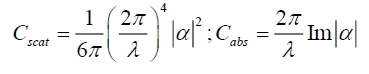
The basic principle for the functioning of plasmonic SCs includes scattering and absorption of light due to the deposition of metal nanoparticles. A thin semiconductor sheet does not absorb light very well. For this reason, more light needs to be scattered across the surface in order to increase the absorption of semiconductor material to convert it into the useful electrical energy [12,13]. It has been found that metal nanoparticles help to scatter the incoming light across the surface of the semiconductor substrate at resonance wavelengths. The scattering and absorption cross-sections are given by:
 (1)
(1)
 (2)
(2)
Where α is the polarizability of the particle, V is the particle volume, εp is the dielectric function of the particle and εm is the dielectric function of the embedding medium. If εp=-2εm, the particle polarizability will become very large. This occurs when the frequency is close to the surface plasmon resonance ωsp, allowing the light to interact over an area larger than the geometric cross section of the particle [14]. In the case of a spherical structure the surface plasmon occurs at ωsp=√3ωsp.
The plasmonic particles improve the light absorption in the semiconductor by three mechanisms. Firstly, by placing the particles on the top of solar cell, the light will be forward scattered into semiconductor at LSPR. Secondly, the particles can scatter light into waveguide modes of the structures, which results in an increased path length [15-17]. Third, light can be trapped locally at LSPR that leads to high field intensities over small volume of the cell. In order to get maximum absorption in the semiconductor layer, the size and shape of scattering particles can be varied. Further, the resonant frequency can be shifted by changing the dielectric constant for the embedding medium in the desired electromagnetic spectrum [10]. In the plasmonic materials of interest, gold shows resonance frequency in visible range and is highly stable, also have broader resonance peak. Although, silver and aluminum are cheap as compared to gold but gets oxidized, which affects resonance frequency. Copper is cheaper than silver and more absorbent than gold. Hence, different materials with various shapes and size can be used to enhance the efficiency of thin film solar cells.
Plasmonic solar cells
Plasmonic solar cells (PSC) are a type of thin film solar cells having thickness of 1 μm to 2 μm (Figure 1). Plasmonic solar cells improve optical absorption by scattering light using metal nanoparticles of different material and configurations excited at their localized surface plasmon resonance (LSPR). The two mechanisms responsible in plasmonic solar cells are electric field enhancement and light scattering enhancement from metal nanoparticles [18-20]. In electric field enhancement, there is strong interaction between light and metal nanoparticles, which leads to increase in the electromagnetic field around the particles. The particles effectively concentrate the light into small regions.

Figure 1: Plasmonic solar cell (PSC).
If a semiconductor is close to or surrounding the metal particles, this will increase the light absorbed by the semiconductor in that region. In light scattering enhancement, the light traps into the solar cell and get reflected by the bottom of the cell, this reflected light is further scattered into the semiconductor medium by metal nanoparticles placed on its surface i.e., the total path length or light trapping is enhanced in the semiconductor materials [21-23]. The design of metallic nanostructures for plasmonic thin film solar cells have received renewed interest lately due to the availability of new nanofabrication tools and better understanding of their optical properties [24-27]. Plasmonic nanoparticles can be integrated with a solar cell in three different geometries. (1) Nanoparticles at the top of the solar cell (Figure 2a). (2) Embedded in the semiconductor (Figure 2b). (3) At the bottom of the semiconductor [28] (Figure 2c). Plasmonic Solar cells can also use multiple physical configurations (multi-junctions) to take advantage of various absorption and charge separation mechanisms (Figure 3). To date, a variety of possible enhancement mechanisms of light trapping are being examined in almost all kind of thin film solar cells with nanoparticles such as silicon based solar cell [25], GaAs solar cell [27], CdSe solar cells [29] and it is also shown that by adjusting the surface plasmon resonance properties, a good broadband antireflection layers are developed [30-32].

Figure 2: Plasmonic light trapping geometries in thin film solar cells.

Figure 3: a) Multijunction plasmonic solar cell.
Recent advancements in PSCs
Incorporation of plasmonic nanostructures into thin-film solar cells has been extensively discussed in recent years. Pillai et al. [25] investigated that absorption of thin film c-Si solar cells can be enhanced by silver nanoparticles of small diameters less than 30 nm. They showed smaller silver metal nanoparticles can provide the maximum overall enhancement in visible and near-infrared region. The scattering of light from a single silver or gold nanoparticles with different material of nanoparticles, shape, size, and dielectric environment was theoretically studied [33] and showed that path length enhancements are higher in cylindrical and hemispherical nanoparticles is higher than spherical nanoparticles. Further, path length enhancement for silver nanoparticles is much higher than gold nanoparticles. For absorption enhancement, the distance of nanoparticles from the substrate is an important factor that is related to the excitation of gap modes [34-36].
To study the effect of higher-order modes on the enhancement 3D modeling was used [37]. They used silver nanoparticles for both size and coverage optimization and given two optimal configurations of silver nanoparticles with diameters of 30 nm and 80 nm and showed that optimal coverage was 33% for 30 nm and 11% for 80 nm for silver nanoparticles, respectively.
Ferry et al. [38] report on the design, fabrication, and measurement of ultrathin film a-Si:H solar cells with nanostructured plasmonic back contacts, which demonstrate enhanced short circuit current densities compared to cells having flat or randomly textured back contacts. The primary photocurrent enhancement occurs in the spectral range from 550 nm to 800 nm. They use angle-resolved photocurrent spectroscopy to confirm that the enhanced absorption is due to coupling to guided modes supported by the cell. Spinelli et al. [39] used silver nanoparticle array geometries to study the coupling of light into a crystalline silicon substrate by scattering light. After simulation and optimization, the best impedance matching for a spectral distribution was observed with spheroidal silver nanoparticles 200 nm wide and 125 nm high in a square array with 450 nm pitch on top of a 50 nm thick Si3N4 layer corresponding to the A. M. 1.5 solar spectrum. Horikoshi et al. [40] used silver nanoparticles of parabolic antenna-type and showed that the field intensity of the absorbing layer in a visible wavelength range (over 650 nm) is enhanced due to its simplified shape. Marco Notarianni et al. [41] showed that power conversion efficiency of a bulk heterojunction solar cell can be increased up to 10% by embedded gold nanoparticles.
Sabaeian et al. [42] investigated by putting the nano-strips of different cross sections (triangle, rectangular and trapezoidal) as a grating structure on the top of the solar cells. The waveguide, surface plasmon polariton (SPP), and localized surface plasmon (LSP) modes were evaluated in transverse electric (TE) and transverse magnetic (TM) polarizations by exciting them with the help of nano-strips. TM modes are more effective than TE modes in optical and electrical properties enhancement of solar cell. The optical absorption, generation rate, and short-circuit current density enhancement for trapezoidal nano-strips showed noticeable impact than triangle and rectangular ones. Zhou et al. [43] used different kinds of solar cells, such as amorphous silicon (a-Si) thin film solar cells, crystalline silicon (c-Si), organic solar cells, single nanowire solar cells and nanowire array solar cells and reviewed various current approaches.
An experimental work by Park et al. [44] used optimized plasmonic silver nanoparticles and polycrystalline silicon thin film solar cells showed increased photocurrent of ~45%. Without a back reflector their absolute efficiency was 5.32% and with the back reflector was 5.95% which are the highest efficiency for metalized plasmonic solar cells reported to date [45]. Nanodisks [46], nanospheres [47,48], nanoplates [49] and nanowires [50]. Ferry et al. [51] used thin film Si and GaAs solar cells using a back interface coated with a corrugated metal film and reported their findings that sub-wavelength scatterers can couple sunlight into guided modes. Pala et al. [52] optimized the Ag strip geometries and reported that they could simultaneously take advantage of both effective coupling to waveguide modes of the semiconductors and high near-field concentration close to their SPs resonance frequency. Munday et al. [53] showed that optimized integrated structure can result in a 1.8-fold total integrated current improvement by combining plasmonic gratings with traditional antireflection coatings together under A. M. 1.5 G solar illumination.
Muhammad et al. [54] studies the effects of the structure geometrical parameters on the absorption and showed that 35% absorption improvements are achieved over the conventional thin film solar cell without metallic nanoparticles. Zhang et. al. [55] simulated low cost and earth abundant Al nanoparticles found 28.7% photon absorption enhancement as compared to noble metal nanoparticles Ag and Au. Further, Al nanoparticles once combined with SiNx anti-reflection coating can produce a 42.5% enhancement which is 4.3% higher than standard SiNx due to the increased absorption in both visible and near- infrared regions. Zhang et al. [56] investigated surface plasmon resonance enhanced optical absorption in thin film Si solar cells with 3 × 3 array of Al nanoparticles and reported 40% absorption enhancement.
Summary
Plasmonic nanostructures incorporation into the thin film solar cells shows special promise both to enhance efficiency of solar cells over a large range of the electromagnetic spectrum and reduce the manufacturing cost. The plasmonic efficiency enhancement depends mainly on the geometrical configuration of metal nanoparticles. The enhancement is induced by the aggregation state which can generate the corresponding plasmon resonance. Further, plasmonic thin film solar cells would help to preserve the environment and provide a wide array of commercial applications due to its wireless capabilities.
References
- Dotan H, Sivula K, Grätzel M, et al.Probing the photoelectrochemical properties of hematite (α-Fe2O3) electrodes using hydrogen peroxide as a hole scavenger. Energy Environ Sci. 2011;4(3):958-64.
- Chander S,Purohit A, Nehra A, et al.A Study on spectral response and external quantum efficiency of mono-crystalline silicon solar cell. IntJRenewEnergy Res. 2015;5(1):41-4.
- VermaSS. Plasmonic solar cells. Renew Energy AkshayUrja.2013;7:22-6.
- Catchpole KR,Polman A.Plasmonic solar cells. Opt Express. 2008;16(26):21793-800.
- Sethi VK, Pandey M, Shukla P.Use of nanotechnology in solar pv cell. IntJChemEngAppl. 2011;2(2):77-80.
- Fraunhofer Institute for Solar Energy systems: Photovoltaic Rep. 2014;18-29.
- Green MA. Third Generation Photovoltaics. Heidelberg: Springer-Verlag, Germany; 2003.
- Atwater HA,Polman A. Plasmonics for improved photovoltaic devices.Nat Mater. 2010;9:205-13.
- Stuart HR, Hall DG.Island size effects in nanoparticle-enhanced photodetectors. Appl Phys Lett. 1998;73(26):3815-17.
- Keely KL, Coronado E, Zhao LL, et al.The Optical Properties of Metal Nanoparticles: The Influence of Size, Shape, and Dielectric Environment. J Phys Chem B. 2003;107(3):668-77.
- Xu G, Tazawa M, Jin P, et al.Wavelength tuning of surface plasmon resonance using dielectric layers on silver island films. ApplPhysLett. 2003;82:3811.
- Bohren CF, Huffman DR. Absorption and scattering of light by small particles. New York: Wiley, USA; 1983.
- Islam K, Alnuaimi A, KemelOkyayA,et al.Improved efficiency of thin film a-Si:H solar cells with Au nanoparticles. 39thIEEE Photovoltaic Specialists Conference; 2013 Jun 16-21, Tampa, Florida, USA; New Jersey:IEEE; 2014. p.1873-76.
- Bohren CF.How can a particle absorb more than the light incident on it? Am J Phys. 1983;51:323-27.
- Green MA. Solar cells: Operating Principles, Technology and system applications.New Jersey: Prentice-Hall, USA;1982.
- Yablonovitch E, Cody GD. Intensity enhancement in textured optical sheets for solar cells. IEEE Trans Electron Dev. 1982;29:300-5.
- Deckman HW, Roxlo CB, Yablonovitch E.Maximum statistical increase of optical absorption in textured semiconductor films. Opt Lett. 1983;8(9):491-93.
- Polman A.Plasmonics Applied. Science. 2008;322(5903):868-9.
- Ferry VE, MundayJN,Atwater HA.Design Considerations for Plasmonic Photovoltaics. Adv Mater.2010;22(43):4794-808.
- Maier SA.Plasmonics: Fundamentals and Applications.New York: Springer, USA; 2007. 224 p.
- Chen X, Jia B, Zhang Y, et al. Exceeding the limit of plasmonic light trapping in textured screen-printed solar cells using Al nanoparticles and wrinkle-like graphene sheets. LightSciAppl. 2013;2:e92.
- Beck FJ, Mokkapati S, Polman A, et al. Asymmetry in photocurrent enhancement by plasmonic nanoparticle arrays located on the front or on the rear of solar cells.Appl Phys Lett. 2010;96(3):033113.
- Beck FJ, Verhagen E, Mokkapati S, et al.Resonant SPP modes supported by discrete metal nanoparticles on high-index substrates. Opt Express. 2011;19(102):A146-56.
- Derkacs D, Lim SH, Matheu P, et al.Improved performance of amorphous silicon solar cells via scattering from surface plasmon polaritons in nearby metallic nanoparticles. Appl Phys Lett. 2006;89:093103.
- Pillai S, Catchpole KR, Trupke T, et al.Surface plasmon enhanced silicon solar cells. J Appl Phys. 2007;101(9):093105.
- Schaadt DM, Feng B,Yu ET.Enhanced semiconductor optical absorption via surface plasmon excitation in metal nanoparticles. Appl Phys Lett. 2005;86:063106.
- Nakayama K, Tanabe K, Atwater HA.Plasmonic nanoparticle enhanced light absorption in GaAs solar cells. Appl Phys Lett. 2008;93:121904.
- Campbell P,Green MA.Light trapping properties of pyramidally textured surfaces. J Appl Phys. 1987;62(1):243-9.
- Konda RB, Mundle R, Mustafa H, et al.Surface plasmon excitation via Au nanoparticles in n-CdSe?p-Si heterojunction diodes. Appl Phys Lett. 2007;91(19):191111.
- Kluth O, Recha B, Houbena L, et al. Texture etched ZnO:Al coated glass substrates for silicon based thin film solar cells. Thin Solid Films 1999;351:247-53.
- Muller J, Rech B, Springer J, et al. TCO and light trapping in silicon thin film solar cells. Solar Energy. 2004;77:917-30.
- Richards BS.Comparison of TiO2 and other dielectric coatings for buried?contact solar cells: a review. ProgrPhotovoltaicsResAppl. 2004;12(4):253-81.
- Catchpole KR, Polman A.Design principles for particle plasmon enhanced solar cells. Appl Phys Lett. 2008;93(19):191113.
- Akimov YA, Ostrikov K, Li EP.Surface Plasmon Enhancement of Optical Absorption in Thin-Film Silicon Solar Cells. Plasmonics. 2009;4(2):107-13.
- Sreekanth KV, Sidharthan R, Murukeshan VM.Gap modes assisted enhanced broadband light absorption in plasmonic thin film solar cell. J Appl Phys.2011;110(3):033107.
- Xu R, Wang X, Song L, et al.Influence of the light trapping induced by surface plasmons and antireflection film in crystalline silicon solar cells. Opt Express. 2012;20(5):5061-8.
- Akimov YA, Koh WS, Ostrikov K. Enhancement of optical absorption in thin-film solar cells through the excitation of higher-order nanoparticle plasmon modes. Opt Express. 2009;17(12):10195-205.
- Ferry VE, Verschuuren MA, Li HB et al.Light trapping in ultrathin plasmonic solar cells. Opt Express. 2010;18(S2):A237-45.
- Spinelli P, Hebbink M, de Waele R, et al.Optical impedance matching using coupled plasmonic nanoparticle arrays.Nano Lett. 2011;11(4):1760-5.
- Horikoshi S, Matsumoto N, Omata Y, et al.Growth of Au nanoparticle films and the effect of nanoparticle shape on plasmon peak wavelength. J Appl Phys. 2014;115(19):193506.
- Notarianni M, Vernon K, Chou A, et al.Plasmonic effect of gold nanoparticles in organic solar cells. Solar Energy. 2014;106:23-37.
- Sabaeian M, Heydari M, Ajamgard N.Plasmonic excitation-assisted optical and electric enhancement in ultra-thin solar cells: the influence of nano-strip cross section. AIP Adv. 2015;5(8):087126.
- Zhou K, Guo Z, Liu S, et al.Current approach in surface plasmons for thin film and wire array solar cell applications. Materials. 2015;8(7):4565-81.
- Varlamov S, Rao J, Soderstrom T.Polycrystalline silicon thin-film solar cells with plasmonic-enhanced light-trapping. J Vis Exp. 2012;(65):4092.
- Park J, Rao J, Kim T, et al. Highest Efficiency Plasmonic Polycrystalline Silicon Thin-Film Solar Cells by Optimization of Plasmonic Nanoparticle Fabrication. Plasmonics. 2013;8(2):1209-19.
- Wu B, Liu X, Oo TZ, et al. Resonant aluminum nanodisk array for enhanced tunable broadband light trapping in ultrathin bulk heterojunction organic photovoltaic devices. Plasmonics. 2012;7(4)677-84.
- Yoon W, Jung KY, Liu J, et al.Plasmon-enhanced optical absorption and photocurrent in organic bulk heterojunction photovoltaic devices using self-assembled layer of silver nanoparticles. Solar Energy Mater Sol Cells. 2010;94(2):128-32.
- Ravi A, Luthra A, Teixeira FL, et al.Tuning the plasmonic extinction resonances of hexagonal arrays of Ag nanoparticles. Plasmonics. 2015;10(6):1505-12.
- Wang DH, Kim JK, Lim GH, et al.Enhanced light harvesting in bulk heterojunction photovoltaic devices with shape-controlled Ag nanomaterials: Ag nanoparticles versus Ag nanoplates. Royal SocChem Adv.2012;2(18):7268-72.
- Kim CH, Cha SH, Kim SC, et al.Silver Nanowire Embedded in P3HT:PCBM for High-Efficiency Hybrid Photovoltaic Device Applications. ACS Nano. 2011;5(4):3319-25.
- Ferry VE, Sweatlock LA, Pacifici D, et al.Plasmonic nanostructure design for efficient light coupling into solar cells. Nano Lett. 2008;8(12):4391-7.
- Pala RA, White J, Barnard E, et al.Design of plasmonic thin?film solar cells with broadband absorption enhancements. Adv Mater. 2009;21(34):3504-9.
- Munday JN, Atwater HA.Large integrated absorption enhancement in plasmonic solar cells by combining metallic gratings and antireflection coatings. Nano Lett. 2010;11(6):2195-201.
- Muhammad MH, Hameed MFO, Obayya SSA.Broadband absorption enhancement in periodic structure plasmonic solar cell. Opt Quant Electron. 2015;47(6):1487-94.
- Zhang Y, Ouyang Z, StokesN, et. al.Low cost and high performance Al nanoparticles for broadband light trapping in Si wafer solar cells. Appl Phys Lett. 2012;100(15):151101.
- Zhang, D, Yang X, Hong X, et al. Aluminum nanoparticles enhanced light absorption in silicon solar cell by surface plasmon resonance. Opt Quant Electron. 2015;47(6):1421-27.