Original Article
, Volume: 14( 13)Synthesis of Organic Polymers Layers Used in Light Emitting Diode (LED) and Studying its Optical and Electrical Properties
- *Correspondence:
- Al Yamani K , Department of Physics, College of Science, Aleppo University, Aleppo, Syria, Tel: 963 938 386 719; E-mail: alyamani.k@gmail.com
Received: July 11, 2016; Accepted: July 17, 2016; Published: August 30, 2016
Citation: Batal MA, Al Yamani K. Synthesis of Organic Polymers Layers Used in Light Emitting Diode (LED) and Studying its Optical and Electrical Properties. Mater Sci Ind J. 2016;14(13):101.
Abstract
Transparent Conductive Oxide/Polyaniline (TCO/PANI) and Transparent Conductive Oxide/Electrolyte Layer/Polyaniline (TCO/EL/PANI) matrix were prepared. Their optical properties reveal a wide band absorption spectrum, PL spectrum have a wide range of emission spectrum in blue region. Electrical properties of DC measurement show low junction series resistance of prepared matrix at room temperature (Rs ≈ 34.96 Ω for TCO/PANI and 23.64 Ω for TCO/EL/PANI). Ideal factor and reverse saturation current were determined at room temperature and found to be (n=10.36, I0=2.13 mA for TCO/PANI and n=8.68, I0=2.1 mA for TCO/EL/PANI). Dimension of electrical conductivity for the prepared matrix sample (TCO/PANI) found to have three-dimensional hopping electrical transport, other parameters calculated as Mott’s characteristic temperature T0 and electrical conductivity (T0=4.58 × 10⁶ K and σ0=843.36 (Ω.m)-1) hopping distance and hopping energy were calculated Rhop=33.34 Å, Whop=71.9 meV respectively.
Keywords
Hopping conductivity; Electrical conductivity; PANI; EL; LED
Introduction
In the past few years, organic-inorganic nanocomposites have become the most interesting field of research for their superior physical properties. This property can be used to make hybrid quantum dots (QDs) organic polymer light emitting diodes (OLEDs) that combine the emitting properties of QDs with the flexibility in device constructed of the organic and polymer materials [1-4]. Polymer-semiconductor nanocomposites generate a new field for the development of advanced materials in science and technology specially industry LEDs which has been demonstrated and is attracting increasing interest in an effort to obtain devices that combine the advantages of both systems for monochromatic visible and near infrared emission as well as for creating white light. Despite recent progress, device efficiencies of QD-LEDs still lag behind the more common organic and polymer LEDs [5]. The properties of the nanocomposites are quite different from the constituent materials due to interfacial interactions between nanostructured semiconductors and polymers. The properties of these materials can easily be tuned to its desired application through the variation of particle size, shape and distribution of nanoparticles. Semiconductor nanoparticles have attracted much interest due to their fundamental as well as technological importance [6,7]. Conducting polymers are widely used as host matrix in the preparation of nanocomposites. Polyaniline (PANI) is one of the most studied conducting polymers because of its good electrical conductivity, environmental stability and relative easy synthesis [8]. The growth of polymer in the presence of inorganic materials strongly affects microstructure of the polymer. The morphology of polymer and interface between polymer and nanoparticle determine the electrical properties of nano composites [9]. High quality colloidal core-shell semiconductor nano crystals, or quantum dots (QDs), offer tunable narrow and intense photoemission as function of size in the visible range because of the spatial confinement of the excited charge carriers [10].
Two types of QD-LED architectures can be discriminated. In the first device lay out, a thin QD layer is sandwiched between a hole and electron injection layer such that excitons are formed directly in the QD layer. In the second layout, the active layer consists of a blend of QDs dispersed in a polymer or small molecule matrix. The QDs in this composite material serve as emissive traps for (migrating) excitons that are generated in the polymer matrix by charge carrier recombination. The use of such hybrid system where the QDs are embedded in a polymer matrix generally gives low luminance efficiency (~0.05 cd/A) for monochromatic devices but was recently reported to be 2.2 cd/A for white-light-emitting devices. In these QD-LEDs, the QD electroluminescence (EL) originates either from recombination of injected charges in the host followed by Forester’s energy transfer to the QD, or by direct trapping and recombination of injected charge carriers on the QDs. In photoluminescence (PL), on the other hand, no (or few) free charge carriers are created in the host after photo excitation and QD emission mainly stems from Forester’s energy transfer from the host, or from direct excitation of the QD. An in-depth study on energy transfer and carrier trapping differences in PL and EL in QD/polymer composite LEDs can contribute to the improvement of hybrid QD LEDs [11]. To increase intensity of emission light and efficiency of PL spectra of transport hole or electrons layer insert between electrode and (P or N) semiconductor layer. In this paper, optical and electrical properties studied for TCO/PANI and TCO/EL/PANI matrix to show influence of electrolyte layer (EL) on TCO/PANI properties.
Materials and Methods
Microscopic slices, K2Cr2O7, glass slides, HF (fluoric acid), SnCl2.2H2O, ethylene glycol, polyaniline (PANI), polyvinyl alcohol (PVA), CuCl2, KI and deionized water were used.
Synthesis of matrix: TCO/PANI-TCO/EL/PANI
Preparing transparent conductive oxide (TCO): Microscopic slice was cleaned using K2Cr2O7. Then it was emerged in diluted fluoric acid (HF) for 10 min to scratch external surface of microscopic slice. After that microscopic slices were heated in electrical oven to 500°C. SnCl2.2H2O (5 g) dissolved in 20 ml of ethylene glycol and sprayed on microscopic slices several times each 5 min. The deposited resistance film SnO2 measured and its 13 Ω to 40 Ω.
Preparing electrolyte layer (EL): PVA powder (5 g) was dissolved in 100 ml of deionized water and stirred with magnetic stirrer at 70°C for 2 h. Previous solution was aged for 1 h at room temperature called solution A. CuCl2.2H2O (5 g) was dissolved in 100 ml of deionized water at room temperature called solution B. Five grams KI was dissolved in 100 ml of deionized water at room temperature called solution C. Solution B measured for 10 ml and was added to 30 ml solution A with keep maxing for 1 h at room temperature. Then solution C was added to previous solution 2 h later drop wise into the reaction vessel satisfying the ratio C=KI/CuCl2 (C=10), followed by stirring for another 2 h. The production process of CuI was according to the following reaction:
2Cu+2+4I– → 2CuI+I2
Preparing TCO/EL/PANI-TCO/PANI matrix: Using spin coating method, TCO/EL/PANI-TCO/PANI matrix was prepared as shown in Figure. 1.

Figure 1: Different matrix (a) TCO/PANI/Ag, (b) TCO/EL/PANI/Ag.
Optical properties
Absorption spectrum of TCO/PANI matrix: Absorption spectra of TCO/PANI matrix carried out using spectrophotometer (UV Win5 V5.2.0). Figure 2 shows TCO/PANI absorption spectrum it reveals many peaks in wavelength range 300 nm to 575 nm. The broad absorption spectrum at ~617 nm is related to π-π* transition. The absorption peak at ~268 nm and ~327 nm arises due to π-π* transition within the benzenoid segment which is associated to the extent of conjugation between adjacent phenyl rings in the PANI [12].

Figure 2: Absorption spectra of TCO/PANI matrix.
PL spectrum of TCO/PANI matrix: Photoluminescence was carried out using spectrophotometer type Hatchi-L250.Figure 3a shows PL spectrum of TCO/PANI photoluminescence (PL) immediately after preparation at room temperature after preparation immediately and Figure 3b shows PL the same matrix one month aged. Both spectra are localized in the blue green region of visible spectrum which originated due to the π-π* transition of the benzenoid unit of PANI [12]. The aged sample give a wide band spectrum centered at 360 nm with displacement about 60 nm toward short wavelength. The difference in intensities between samples is due to thickness of aged sample.

Figure 3: a) PL spectra of TCO/PANI matrix aged for 30 days, b) PL spectra of TCO/PANI matrix after preparation.
PL spectrum of TCO/EL/PANI matrix: Figure.4 reveals four peaks of PL spectrum of matrix TCO/EL/PANI measured at room temperature, the most PL intensity peak located at 399.2 nm which was narrow that means small size distributions of nanoparticles of matrix.

Figure 4: PL spectra of TCO/EL/PANI matrix.
Electrolyte layer, which inserted between TCO/PANI layers change PL spectra of matrix from a wide PL spectrum to district spectrum, have three narrow peaks and PL intensity decrease from 340 a.u to 243 a.u as shown in Figure.4. This is due to electrolyte layer, which has high carrier charge intensity.
Electrical properties
Current versus voltage characterization: Current-voltage characteristic measured using millimeter type keitithley (28775). Figure.5 shows (I-V) characteristics of the matrix samples measured at room temperature. It reveals that (I-V) characteristics linear for forward and reverse bias voltage. This suggests that Schottky barriers are formed in the nanocomposites. The applied forward bias voltage and the current based on thermionic emission current fit well with the following equation [13]:

Figure 5: I-V Characterization of (a) TCO/PANI matrix (b) TCO/EL/PANI matrix.
 (1)
(1)
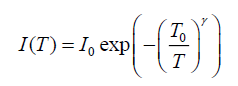
Where I0 is saturation current, T0 is Mott’s characteristic temperature associated with the degree of localization of the electronic wave function. The exponent γ=1/(1+d) determines the dimensionality (d) of the conducting medium.
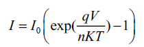
Reverse saturation current and junction ideality factor: At low voltages (V ≤ 0.5 V), the current varies exponentially with voltage and can be fitted to Shockley equation [14]:
 (2)
(2)
By taking logarithm of two sides:
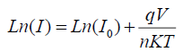
where q is electron charge, I0 is reverse saturation current, n is junction ideality factor, K is Boltzmann constant and T is absolute temperature. From previous equation, it is evident that from the y-intercept and slope of the semi-log I-V plot (Figure.6). One can extract the reverse saturation current and ideality factor, respectively. Ideality factor and reverse saturation currents were found to be (n=10.36, I0=2.13 mA for TCO/PANI and n=8.68, I0=2.1 mA for TCO/EL/PANI at room temperature.

Figure 6: Dark current-voltage characteristics plotted as semi-log at room temperature.
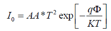
I0 is the saturation current and defined by [14]:
 (3)
(3)
Where the quantities A, A*, T, q, k and Φ are the area, the effective Richardson constant, temperature in Kelvin, the electronic charge, Boltzmann constant and the apparent barrier height respectively.
Differential resistance of TCO/PANI-TCO/EL/PANI matrix: Shunt resistance Rsh and series resistance Rs are important parameters for matrix performance. Junction resistance e.g. rate of change of voltage with respect to current when plotted as a function of voltage as shown in Figure.7.

Figure 7: Dependence of junction resistance on voltage at room temperature.
It helped to determine series resistance Rs ≈ 34.96 Ω for TCO/PANI-23.64 Ω for TCO/EL/PANI (as minima of curve) and shunt resistance R ≈ 49.83 Ω for TCO/PANI-40.65 Ω for TCO/EL/PANI (as maxima of curve) of the curve. Low series resistance reflects low resistivity of these matrix thin films.
Conduction mechanisms: Conduction mechanism may be explained as follows: at lower voltages, current is directly proportional to voltage showing Ohmic conductive region due to thermally generated carriers. The current density J in Ohmic region is expressed as [15]:
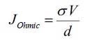 (4)
(4)
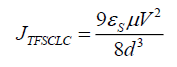
Where σ is the electrical conductivity, d is thickness of matrix and V is the applied voltage. At higher voltages (V>0.4 V) the current depends on the applied voltage according to the power law J ∝ Vm where m ≥ 2, typical of a Space Charge Limited Current (SCLC) conduction mechanism. The forward bias refers to whole injection of anode into the Highest Occupied Molecular Orbital (HOMO) of EL/PANI matrix and reverse bias refers to the electron injection of cathode into the conduction band of matrix Low Unoccupied Molecular Orbital (LOMO). The Sliver (Ag) electrode forms a relatively low barrier (Ohmic contact) with TCO. Therefore, at low voltages, the overall behavior becomes Ohmic due to low density of injected holes. With the increase in voltage, the injected whole density increases and ultimately surmounts the transport capacity of matrix EL/PANI, hence positive space charge accumulates near the anode. The field due this space charge dominates over the applied field and is responsible for limiting the current and giving rise to space-charge limited current (SCLC) conduction. SCLC takes place when extra injected carriers have a transit time which is less than the bulk relaxation time [16], in other words the injection rate of excess charges exceeds the rate at which the charges are being swept to the collecting electrodes due to low mobility [17]. In general, variation of current with voltage can be described as: I ∝ Vm from previous relation the following equation can be easily derived: log(I) ∝ m log(V) it is evident that from the slope of the double-log I-V plot, Log I vs Log V as shown in Figure.8, Ohmic and SCLC regions can be identified. In region-II, slope of the curve is approximately unity indicating Ohmic conduction due to thermally generated charge carriers whereas region-I with slope approximately (quadratic dependence of the current on voltage) indicates trap free space-charge limited current (TFSCLC) conduction [17]. Due to low mobility of organic semiconductors, the excess charges are not swept to the collecting electrodes with the same rate at which they are injected. Therefore, it is important to realize that slope of approximately 2 does not necessarily justify the absence of traps in the material. Under these conditions, the space charge limited current (TFSCLC) flows, as given by [16]:
 (5)
(5)

Figure 8: Dark current-voltage characteristics plotted on double-log at room temperature.
Where μ is mobility, (εs=εrε0) is the static relative dielectric constant of organic matrix. εs ≈ 6.89 ε0 for PANI, d is thickness of matrix. It is thought that the trap states, because of various lattice imperfections and impurity sites that might have been created in the organic thin film during thermally evaporation [18]. Region-III with slope above 2 indicates SCLC conduction mode dominated by the traps distributed exponentially with energy within the band gap of the PANI. For this region, current density can be given by Child’s law [19]:
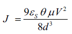
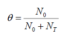
Where θ represents the trapping factor, describe as the ratio of free hole/electron carrier density N0 to the total carrier density N0+NT, where NT is trapped charge density. Trap factor is given as:
 (6)
(6)
Determines dimensionality of the conducting medium: The temperature dependence of conductivity for TCO/PANI matrix is shown in Figure.9. The temperature dependence of conductivity G(T) is analyzed by Mott's variable range hopping (VRH) model [11]:
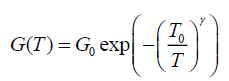 (7)
(7)
Where G0 is the high temperature limit of conductivity and T0 is Mott’s characteristic temperature associated with the degree of localization of the electronic wave function.
The exponent γ=1/(1+d) determines the dimensionality of the conducting medium. The possible values of γ are ¼, ? and ½ for three, two and one-dimensional systems respectively. The best-fitted value of γ is obtained by the linear regression analysis as reveal Figure.9. The lowest standard deviation was found for γ=1/4 for TCO/PANI matrix. That means three dimensionality of the conducting medium. The values of Mott’s characteristic temperature T0 and the pre-exponential factor σ0 are obtained from the slopes and intercepts of Figure.10. The values of T0=4.58 × 10⁶ K and σ0=843.36 (Ω.m)-1. The characteristic temperature T0 for three-dimensional hopping transport is given by [11]:
 (8)
(8)

Figure 9: a) Ln(I) in terms of 1/T of TCO/PANI, b) Ln(G) in terms of 1/T of TCO/PANI matrix.

Figure 10: C-V characterization of TCO/PANI matrix (a), TCO/EL/PANI matrix (b).
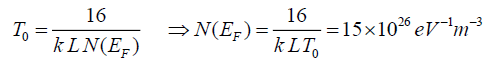
Where L is the localization length and N(EF) is the density of states at the Fermi level and as T0 is inversely proportional to L, the degree of disorder of the systems reduces with lowering of T0. Electrical conductivity of TCO is very low due to large band gap compared to PANI matrix. Electrical conduction in nano composites occurs mainly through conductive paths of PANI. The values of N(EF) are calculated by considering the charge transport primarily arising from conducting PANI phase and assuming localization length of the polyaniline monomer unit about 3A. It is clear that the value of N(EF) may increase with increasing PANI content [13]:
 (9)
(9)
 (10)
(10)
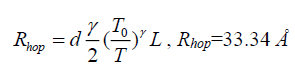
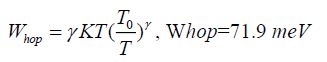
Increase of density of states and decreases of hopping distance and hopping energy enhance the conductivity of nano composites.
Capacitance versus voltage characterization: C-V characteristic measurements carried out at room temperature and constant frequency (100 Hz) carried out using RLC type MICROTEST (6379). Figure.10 showed constant capacitance for TCO/EL/PANI matrix until voltage 0.8 v like PN junction. Voltage up 1 V capacitance decreases with increasing voltage this behavior like varactor diode.
Capacitance of TCO/PANI matrix increase with increasing applied voltage up to 416 mV and then start to decrease with increasing applied voltage.
Deep trapped charge contribution: Contribution estimation of deep trapped charge density in TCO/EL/PANI matrix can be estimated from measuring the capacitance C in function of frequency logarithm. Figure.11 shows the relationship between capacitance C and Log (f) in range frequency (20 Hz to 2 KHz). Figure.11 reveals that there are two capacitors in series at low frequencies from 20 Hz to 100 Hz. Capacitance decreases from value (C1Total=25.93 nF to CS=18.85 nF) that means carrier charge contribution decreases rapidly. This means there are two kinds of charges (surface and deep trapped charge) contribute in charge capacitance. At higher frequency (100 Hz up to 1200 Hz) capacitance decrease also to new value (C2total=14.03 nF) that means there are two trap levels in TCO/EL/PANI matrix contribute to the capacitance charge. At low frequencies there are contributions of deep carrier due to the high relaxation time (low frequency), carrier charge has enough time to relax and appear on electrodes capacitance. The total capacitance at low frequency can be written:
-characterization-14-13-101-g011.png "materials-science-C-Log(f)-characterization")
Figure 11: C-Log(f) characterization of TCO/EL/PANI matrix.
Ctot=Ctrap+Cs, CTrap=CTOT–CS
Where, CTrap the capacitance comes from the contribution deep trapped charges, Cs capacitance contributions of surface carrier charge (measured at high frequency, Measured at low frequency).
Conclusion
The prepared matrix has a wide band absorption located in wavelength range 308 nm to 616 nm. PL spectrum of matrix sample has a moderated intensity, which is located in blue region of emissions spectrum. This permits to use this matrix as a layer in quantum dots light emitting diode (QDLEDs). DC measurement indicates electrical properties which makes evident that the shunt resistance is very low.
C-V characteristic shows that there was two regions constant capacitance with applied voltage between 0.1 V to 0.8 V (behavior like ideal semiconductors). The capacitance decreases with increasing applied voltage above 1 V. This characteristic allows QDLEDs to be used as reactor diode.
Conductivity dimension of matrix was three-dimensional hopping transport; hopping distance and hopping energy were calculated and found to be Rhop=33.34 Å, Whop=71.9 meV respectively.
References
- Gangopadhyay R, Amitabha D. Conducting Polymer Nanocomposites. In: Nalwa HS, editor. Handbook of Organic-Inorganic Hybrid Materials and Nanocomposites. California: American Scientific Publishers;2003. p. 217-265.
- Fedorov MI. Organic-inorganic heterostructures and their properties.Ryazan: Ryazan State Technical University; 2004.
- Minaev B, Baryshnikov G, Agren H. Principles of phosphorescent organic light emitting devices. Phys Chem Chem Phys. 2014;16:1719-58.
- CherpakV,Stakhira P, Minaev B,et al. Efficient "Warm-White" OLEDs Based on the Phosphorescent bis-Cyclometalated iridium (III) Complex. J Phys Chem C. 2014;118:11271-8.
- Maennig M, Pfeiffer A. Nollau X, et al. Controlled p-type doping of polycrystalline and amorphous organic layers:Self-consistent description of conductivity and ?eld-e?ect mobility by a microscopic percolationmodel. Phys Rev B. 2001;64:195208.
- Anikeeva PO, Halpert JE, Bawendi MG, et al. Electroluminescence from a mixed red-green-blue colloidal quantum dot monolayer. Nano Lett. 2007;7:2196-200.
- Anikeeva PO, Halpert JE, Bawendi MG, et al. QD-LEDs with electroluminescence tunable over the entire visible spectrum.Nano Lett. 2009;9:2532-36.
- Jang J, Bae J, Lee K. Synthesis and characterization of polyaniline nanorods as curing agent and nanofiller for epoxy matrix composite. Polymer. 2005;46:3677-84.
- Plesu N, Ilia G, Pascariu A, et al. Preparation, degradation of polyaniline dopedwith organic phosphorus acids and corrosion essays of poly aniline-acrylic blends.Synth Met. 2006;156:230-8.
- Lee YL, Lo YS. Highly ef?cient quantum-dot-sensitized solar cell based on Co-sensitization of CdS/CdSe. Adv Funct Mater. 2009;19:604-9.
- Nizamoglu S, Demir HM. Resonant nonradiative energy transfer in CdSe/ZnS core/shell nanocrystal solids enhances hybrid white light emitting diodes. Opt Express. 2008;16(18):13961-8.
- Kondawar SB, Thakare SR. Nanostructure Titania Reinforced Conducting Polymer Composites. Int J Mod Phys B. 2009;23(15):3297-304.
- De SK, Kousik D. Optical and nonlinear electrical properties of SnO2–polyaniline nanocomposites. Mater Lett.2007;61(27):4967-71.
- Sze SM. Physics of Semiconductor Devices, Berlin: John Wiley and Sons; 1981.
- Amar N, Gould RD, Saleh AM. Structural and electrical properties of the a-form of metal-free Phthalocyanine (a-H2Pc) thin films.Curr Appl Phys. 2002;2(6):455-60.
- Abkowitz M, Facci JS, Rehm J. Direct evaluation of contact injection efficiency into small molecule based transport layers: Influence of extrinsic factors.J Appl Phys. 1998;83(5):2670-6.
- Roy MS, Balraju P, Deol YS, et al. Charge transportation and photo generation process in polythiophene functionalized with tin (II) phthalocyanine (SnPc-PT) thin film. Sol Energy Mater Sol Cells. 2008;92(11):1516-25.
- Anthopoulos TD, Shafai TS. Junction Properties of Nickel Phthalocyanine Thin Sandwich Film Structures Using Dissimilar Electrodes. PhysStatus SolidiA.2001;186(1):89-97.
- Kao KC, Hwang W. Electrical Transport in Solids, with Particular Reference to Organic Semiconductors. In: International Series in the Science of the Solid State. Oxford: Pergamon Press; 1981. p. 418-22.