Original Article
, Volume: 10( 6)An Approach to Increase Density of Field-Effect Heterotransistors Framework Circuits NAND and AND
- *Correspondence:
- Pankratov EL , Nizhny Novgorod State University, 23 Gagarin avenue, Nizhny Novgorod, 603950, Russia, Tel: +7 831 245-33-32
E-mail: elp2004@mail.ru
Received: September 09, 2016; Accepted: September 30, 2016; Published: October 08, 2016
Citation: Pankratov EL, Bulaeva EA. An Approach to Increase Density of Field-Effect Heterotransistors Framework Circuits NAND and AND. Nano Sci Nano Technol. 2016;10(6):108.
Abstract
We introduce an approach to increase density of field effect heterotransistors, which include into itself circuits NAND and AND. The approach based on manufacturing a specific configuration of a heterostructure. After the manufacturing, we consider doping of several areas of the heterostructure by diffusion or ion implantation. After the doping, we consider optimized annealing of dopants and generated radiation defects during ion implantation. We consider redistribution of dopant and radiation defects under influence of mismatch induced stress. Some comparison of calculated results with experimental one has been done.
Keywords
Circuits NAND and AND; increasing of density of elements
Introduction
Currently density of elements of integrated circuits is intensively increasing. To obtain the increasing dimensions of the elements should decreased. Presently several methods to decrease the dimensions have been developed. One way to decrease the dimensions is growing thin films structures and manufacturing the above elements framework the structures [1-5]. Another one is using laser or microwave irradiation to anneal dopants or radiation defects [6-9]. Both types of annealing lead to generation in homogenous distribution of temperature. In this situation one can obtain more in homogenous distribution of dopant and consequently more compact elements framework the considered integrated circuits. Another approach to change properties of doped materials is radiation processing [10,11].
Framework the present paper we consider an approach to manufacture smaller field-effect heterotransistors framework circuits NAND and AND. We assume that the considered transistors have been manufactured framework a heterostructure. The heterostructure consist of a substrate and an epitaxial layer. We consider several sections, which were manufactured in the epitaxial layer by using other materials. After that we consider diffusion and ion types of doping to prepare p or n types of conductivity in the considered sections. Now we consider manufacturing a field effect transistors framework the heterostructure with epitaxial layer on Figure.1. Now we consider annealing of dopant (for diffusion type of doping) and radiation defects (for ion type of doping).Main aim of the present paper is optimization of the annealing. The optimization gives a possibility to obtain increasing of density of transistors in these circuits with decreasing their dimensions. We also consider an approach of decreasing of mismatch- induced stress in heterostructure.

Figure 1: Structure of circuits NAND and AND. View from top.
Method of solution
To solve our aim, we calculate spatio temporal distribution of concentration of dopant. We consider the distribution as solution of the following boundary problem [10-14].

with boundary and initial conditions

Here C (x,y,z,t) is the spatio temporal distribution of concentration of dopant; Ω is the atomic volume of the dopant; symbol
ΩS is the surficial gradient;  is the surficial concentration of dopant in neighborhood of the interface
between materials of heterostructure (in this case we assume, that Z-axis is perpendicular to the interface be-tween materials
of heterostructure); μ (x,y,z,t) is the chemical potential; D and DS are the coefficients of volumetric and surficial diffusions
(the surficial diffusion is the consequences of mismatch-induced stress). Values of diffusion coefficients depend on properties
of materials of heterostructure, speed of heating and cooling of heterostructure, concentration of dopant. Dependences of
dopant diffusion coefficients on parameters could be approximated by the following relations [12].
is the surficial concentration of dopant in neighborhood of the interface
between materials of heterostructure (in this case we assume, that Z-axis is perpendicular to the interface be-tween materials
of heterostructure); μ (x,y,z,t) is the chemical potential; D and DS are the coefficients of volumetric and surficial diffusions
(the surficial diffusion is the consequences of mismatch-induced stress). Values of diffusion coefficients depend on properties
of materials of heterostructure, speed of heating and cooling of heterostructure, concentration of dopant. Dependences of
dopant diffusion coefficients on parameters could be approximated by the following relations [12].
 (2)
(2)
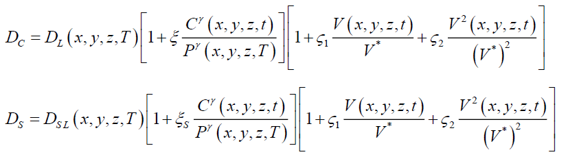
Here DL (x,y,z,T) and DLS (x,y,z,T) are the spatial (due to accounting all layers of hetero-structure) and temperature (due to Arrhenius law) dependences of dopant diffusion coefficients; T is the temperature of annealing; P (x,y,z,T) is the limit of solubility of dopant; parameter γ depends on properties of materials and could be integer in the following interval γ € [1,3] [12], V (x,y,z,t) is the spatio-temporal distribution of concentration of radiation vacancies; V* is the equilibrium distribution of vacancies. Concentration dependence of dopant diffusion coefficient has been described in details in [12] ref. Spatio temporal distributions of concentration of point radiation defects have been determined by solving the following system of equations [11,13,14].
 (3)
(3)

with boundary and initial conditions

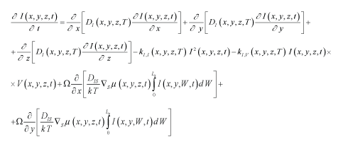
Here I (x, y, z, t) is the spatio-temporal distribution of concentration of radiation interstitials; I* is the equilibrium distribution of interstitials; DI (x, y, z, T), DV (x, y, z, T), DIS (x, y, z, T), DVS (x, y, z, T) are the coefficients of volumetric and surficial diffusions of interstitials and vacancies, respectively; terms V2(x, y, z, t) and I2(x, y, z, t) correspond to generation of divacancies and diinterstitials, respectively [11], kI,V(x, y, z, T), kI,I (x, y, z, T) and kVV (x, y, z, T) are the parameters of recombination of point radiation defects and generation of their complexes.
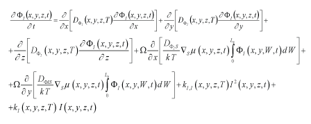
We determine spatio-temporal distributions of concentrations of divacancies ΦV (x, y, z, t) and diinterstitials ΦI (x, y, z, t) by solving the following system of equations [11,13,14].
 (5)
(5)

with boundary and initial conditions

Here DΦI (x, y, z, T), DΦV (x, y, z, T), DΦIS (x, y, z, T) and DΦVS (x, y, z, T) are the coefficients of volumetric and surficial diffusions of complexes of radiation defects kI (x, y, z, T) and kV (x, y, z, T) are the parameters of decay of these complexes. Chemical potential in Eq (1) could be determined by the following relation [13]
 (7)
(7)
where E (z, C) = E1 (z) + E2 (z) [C(x, y, z, t)/P(x,y,z,T)] [15] is the Young modulus, σij is the stress tensor;  is the deformation tensor; ui, uj are the components ux (x, y, z, t), uy (x, y, z, t) and uz (x, y, z, t) of the
displacement vector ; variables xi, xj equal to x, y, z depends on number of equation for components of displacement vector.
The Eq. (7) could be transformed to the following form
is the deformation tensor; ui, uj are the components ux (x, y, z, t), uy (x, y, z, t) and uz (x, y, z, t) of the
displacement vector ; variables xi, xj equal to x, y, z depends on number of equation for components of displacement vector.
The Eq. (7) could be transformed to the following form

Where σ is the Poisson coefficient;  is the mismatch parameter; as, aEL are the lattice distances of the substrate
and the epitaxial layer, respectively; K is the modulus of uniform compression; β is the coefficient of thermal expansion; Tr is
the equilibrium temperature which coincides (for our case) with the room temperature. Components of displacement vector
could be obtained by solution of the following equations [15,16]
is the mismatch parameter; as, aEL are the lattice distances of the substrate
and the epitaxial layer, respectively; K is the modulus of uniform compression; β is the coefficient of thermal expansion; Tr is
the equilibrium temperature which coincides (for our case) with the room temperature. Components of displacement vector
could be obtained by solution of the following equations [15,16]

Here

 p(z) is the density of materials of heterostructure, σij is the Kronecker symbol.
Accounting the above relation for sij in the previous system of equations last system of equation could be written as
p(z) is the density of materials of heterostructure, σij is the Kronecker symbol.
Accounting the above relation for sij in the previous system of equations last system of equation could be written as

Conditions for the system of these equations are

We determine spatio-temporal distributions of concentrations of dopant and radiation defects by solving the Eqs. (1), (3) and (5) simultaneously by the standard method of averaging of function corrections [17,18]. On the first step of solving of our aim we take into account initial distributions of the considered concentrations in the Eqs. (1), (3) and (5). In this situation initial conditions after appropriate equations will be equal to zero. After that we replace the required functions in right sides of Eqs. (1a), (3a) and (5a) on their not yet known average values α1p In this situation, we obtain equations for the first-order approximations of the considered concentrations in the following form
 (1b)
(1b)
 (3b)
(3b)

Integration of the left and right sides of Eqs. (1b), (3b) and (5b) gives us the possibility to obtain relations for above firstorder approximations in the following form
 (1c)
(1c)


We determine average values of the first-order approximations of required functions by using the following relations [17,18]
 (9)
(9)
Substitution of these relations (1c), (3c) and (5c) into relation (9) gives us a possibility to obtain the following relations

Where


Where

Approximations of the above concentrations of the second and higher orders we obtain framework standard iterative procedure of method of averaging of function corrections [17,18]. Framework the procedure to determine approximations with the n-th-order approximations of concentrations of dopant and radiation defects we replace the required concentrations C(x,y,z,t), I(x,y,z,t), V(x,y,z,t), ΦI(x,y,z,t) and ΦV(x,y,z,t) in right sides of Eqs. (1), (4) and (6) on sums of the following sums αnρ+ρn-1(x,y,z,t), where αnρ are the average values of n-th-order approximations of concentrations of dopant and defects ρn-1(x,y,z,t). The replacement leads to the following results


Integration of the left and right sides of Eqs. (1d), (3d), (5d) gives us possibility to obtain relations for the second-order approximations of dopant and radiation defects in the following form

 (1e)
(1e)
 (3e)
(3e)

 (5e)
(5e)

We determine average values of the second-order approximations of required functions by using of the standard relation [17,18]
 (10)
(10)
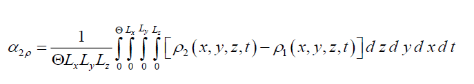
Substitution of the relations (1e), (3e), (5e) into relation (10) gives us possibility to obtain relations for the parameter α2ρ

where

After that we determine solutions of the system of Eqs. (8). The solutions physically correspond to components of displacement vector. To determine components of displacement vector we used the method of averaging of function corrections in its standard form. By using this approach, we replace the above components in right sides of Eqs. (8) by their not yet known average values αi. The substitution leads to the following results.

Integration of the left and right sides of the above equations on time t leads to final relations for the first-order approximations of components of displacement vector in the following form


Approximations of the second-order and higher orders of components of displacement vector could be calculated by replacement of the required components in the Eqs. (8) by the following sums αI + ui (x, y, z, t) [16,17]. The replacement leads to the following result.


Integration of left and right sides of the above equations on time t leads to the following results


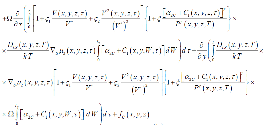
In this paper we determine concentration of dopant, concentrations of radiation defects and components of displacement vector by using the second-order approximations, which were calculated by using method of averaging of function corrections. This approximation is usually good enough approximation to carry out a qualitative analysis and to obtain some quantitative results. Everything obtained analytical results have been checked by comparison with results of numerical simulations. In this paper, we used explicit difference scheme to solve Eqs. (1), (3) and (5).
Discussion
In this section we analyzed dynamics of redistributions of dopant and radiation defects under the influence of mismatch-induced stress during annealing. Typical distributions of concentrations of dopant in heterostructure are presented on Figure 2 and 3 for diffusion and ion types of doping, respectively. These distributions have been calculated for the case, when the value of dopant diffusion coefficient in doped area is larger, than in nearest areas. The figures show, that inhomogeneity of heterostructure gives us a possibility to increase compactness of distribution of concentration of dopant. At the same time one can find increasing homogeneity of dopant distribution in the doped part of epitaxial layer. The effect leads to decreasing local heating of materials during functioning of transistor or decreasing the dimensions of the transistor for fixed maximal value of local overheat. However, applications of this approach of manufacturing of transistor required optimization annealing of dopant and/or radiation defects. The main reason for this optimization is following. If the annealing time is small, the dopant does not achieve any interfaces be-tween the materials of heterostructure. In this situation one cannot find any modifications of the distribution of concentration of dopant. If the annealing time is large, the distribution of concentration of dopant is too homogenous. We optimize the annealing time based on a recently introduced approach [18-26]. By applying this criterion, the criterion, we approximate real distribution of concentration of dopant by a step wise function Figure 4 and 5. Next we determine optimal values of annealing time by minimization of the following mean-squared error.
 (15)
(15)

Figure 2: Distributions of concentration of infused dopant in heterostructure from Fig. 1 in direction, which is perpendicular to interface between epitaxial layer substrate. The increasing number in the curve corresponds to an increase in difference between values of dopant diffusion co-efficient in layers of heterostructure under condition, when the value of dopant diffusion coefficient in epitaxial layer is larger, than value of dopant diffusion coefficient in substrate (D1/D0=1, D1/D0=1.2, D1/D0=1.4, D1/D0=1.6, D1/D0=1.8, D1/ D0=1.999, D1/D0=D0/D2, respectively; Θ=0.01 (Lx2+Ly2+Lz2)/D0; average value of dopant diffusion coefficient is equal to D0=1; D1 and D2 are values of dopant diffusion co-efficient in doped material of heterostructure and in nearest material). Squares are the experimental data from [27]. Circles are the experimental data from [28]. Both experimental data have been obtained for heterostructure.

Figure 3: Distributions of concentration of implanted dopant in heterostructure from Fig. 1. in direction, which is perpendicular to the interface between epitaxial layer substrate. Curves 1 and 3 correspond to annealing time Θ=0.0048 (Lx2+Ly2+Lz2)/D0. Curves 2 and 4 correspond to annealing time Θ=0.0057 (Lx2+Ly2+Lz2)/D0. Curves 1 and 2 correspond to homogenous sample (D1/D0=D0/D2=1). Curves 3 and 4 correspond to heterostructure under condition, when value of dopant diffusion coefficient in epitaxial layer is larger, than value of dopant diffusion coefficient in substrate (D1/D0=D0/D2= 1.2). Squares are the experimental data from [29]. Circles are the experimental data from [30]. Both experimental data have been obtained for homogenous samples.

Figure 4: Spatial distributions of dopant in heterostructure after dopant infusion. Curve 1 is an idealized distribution of dopant. Curves 2-4 are real distributions of dopant for different values of annealing time. The increasing number in the curve corresponds to the increasing annealing time..

Figure 5: Spatial distributions of dopant in heterostructure after ion implantation. Curve 1 is an idealized distribution of dopant. Curves 2-4 are real distributions of dopant for different values of annealing time. The increasing number in the curve corresponds to the increasing annealing time.
Where ψ (x, y, z) is the step-wise approximation of spatial distribution of concentration of dopant C (x, y, z, t). We minimize the mean-squared error as the function of time. After the minimization, we obtain optimal value of annealing time Θ. Dependences of optimal values of annealing time on parameters are presented in Figure 6 and Figure 7. for diffusion and ion types of doping, respectively. It should be noted, that it is necessary to anneal radiation defects after ion implantation. One could find spreading of concentration of the distribution of concentration of dopant during this annealing. In the ideal case distribution of do-pant achieves appropriate interfaces between materials of heterostructure during annealing of radiation defects. If dopant does not achieve to the nearest interface during annealing of radiation defects, it is practical to additionally anneal the dopant. In this situation, the optimal value of the additional annealing time of implanted dopant is smaller, than the annealing time of infused dopant.

Figure 6: Dependences of dimensionless optimal annealing time for doping by diffusion, which have been obtained minimization of mean-squared error, on several parameters. Curve 1 is the dependence of dimensionless optimal annealing time on the relation a/L and ξ= γ= 0 for equal values of dopant diffusion coefficient in all parts of heterostructure. Curve 2 is the dependence of dimensionless optimal annealing time on the value of the parameter ε for a/L=1/2 and ξ= γ= 0. Curve 3 is the dependence of dimensionless optimal annealing time on the value of parameter ξ for a/L= 1/2 and ε = γ= 0. Curve 4 is the dependence of dimensionless optimal annealing time on value of parameter γ for a/L= 1/2 and ε= ξ= 0.

Figure 7: Dependences of dimensionless optimal annealing time for doping by ion implantation, which have been obtained by minimization of mean-squared error, on several parameters. Curve 1 is the dependence of dimensionless optimal annealing time on the relation a/L and ξ = γ = 0 for equal values of dopant diffusion coefficient in all parts of heterostructure. Curve 2 is the dependence of dimensionless optimal annealing time on the value of the parameter ε for a/L=1/2 and ξ= γ= 0. Curve 3 is the dependence of dimensionless optimal annealing time on the value of parameter ξ for a/L= 1/2 and ε = γ = 0. Curve 4 is the dependence of dimensionless optimal annealing time on value of parameter γ for a/L=1/2 and ε= ξ = 0.
Next we analyzed the influence of relaxation of mechanical stress on distribution of do-pant in doped areas of heterostructure. Under following condition ε0<0 one can find compression of distribution of concentration of dopant near the interface between materials of heterostructure. Contrary (at ε0>0) one can find spreading of distribution of concentration of dopant in this area. Accounting relaxation of mismatch-induced stress in heterostructure could leads to changing of optimal values of annealing time.
Farther we compare relaxation of mismatch-induced stress for diffusion and ion types of doping. The Figure 8 shows dependences of component of displacement vector, which is perpendicular to interface between materials of heterostructure, on coordinate. Curve 1 corresponds to diffusive type of doping. Curve 2 corresponds to ion type of doping. Reason of decreasing of mismatch-induced stress is radiation processing of materials during ion implantation [26].

Figure 8: Normalized dependences of perpendicular to interface between materials of heterostructure components of displacement vector uz on coordinate. Curve 1 corresponds to diffusive type of doping. Curve 2 corresponds to ion type of doping.
Conclusion
In this paper, we consider a possibility to increase density of elements in circuits NAND and AND. The circuits manufactured based on field-effect hetero transistors. As an accompanying effect, we consider an approach to decrease mismatch-induced stress.
Acknowledgements
This work is supported by the agreement of August 27, 2013 No 02.B.49.21.0003 between The Ministry of education and science of the Russian Federation and Lobachevsky State University of Nizhni Novgorod and educational fellowship for scientific research of Government of Russia.
References
- Volovich G. Modern chips UM3Ch class D manufactured by firm MPS. Mode Elect. 2006;2:10-7.
- Kerentsev A, Lanin V. Constructive-technological features of MOSFET-transistors. Power Elect. 2008;1:34-8.
- Ageev AO, Belyaev AE, Boltovets NS, et al. Au–TiBx- n-6H-SiC Schottky barrier diodes: the features of current flow in rectifying and nonrectifying contacts. Semiconductors. 2009;43(7):897-903.
- Volokobinskaya NI, Komarov IN, Matioukhina TV, Investigation of technological processes of manufacturing of the bipolar power high-voltage transistors with a grid of inclusions in the collector region. Semiconductors. 2001;35(8)1013-17.
- Subramaniam A, Cantley KD, Vogel EM. Logic Gates and Ring Oscillators Based on Ambipolar Nanocrystalline-Silicon TFTs. Act Pass Elect Comp. 2013;525017.
- Ong KK, Pey KL, Lee PS, et al. Dopant distribution in the recrystallization transient at the maximum melt depth induced by laser an-nealing. Appl Phys Lett. 2006;89(17):172111-4.
- Wang HT, Tan LS, Chor EF. Pulsed laser annealing of Be-implanted GaN. J Appl Phys. 2006;98(9):094901-5.
- Mazhukin VI, Nosov VV, Semler U. Study temperature and thermal stress fields in pulse treatment of semiconductors. Mathematical Modelling. 2000;12(2)75-83.
- Yu VB, Yeremeev AG, Zharova NA, et al. Diffusion processes in semiconductor structures during microwave annealing. Radiophy Quan Elect. 2003;43(3)836-43.
- Kozlivsky VV. Modification of semiconductors by proton beams. Fizika i tekhnikapoluprovodnikov. 2003;34(2):129-47
- Vinetskiy VL, Kholodar GA. Radiative physics of semiconductors. ("NaukovaDumka", Kiev, 1979, in Russian).
- Yu Z. Gotra. Technology of microelectronic devices. Radio commun. Moscow. 1991.
- Zhang YW, Bower AF. Numerical simulations of island formation in a coherent strained epitaxial thin film system. Mechanics Physics Solids. 1999;47(11)2273-97.
- Fahey PM, Griffin PB, Plummer JD. Point defects and dopant diffusion in silicon. Rev. Mod. Phys. 1989;61(2):289-388.
- Landau LD, Lifshits EM. Theoretical physics. 7 (Theory of elasticity) (Physmatlit, Moscow, 2001, in Russian).
- Zhang K, Li Y, Zheng B. Effects of concentration dependent elastic modulus on Li ions diffusion and diffusion-induced stresses in spherical composition-gradient electrodes. J Appl Phys. 2015;118 (10)1051021-9.
- Sokolov YD. About the definition of dynamic forces in the mine lifting. Appl Mecha. 1955;1(1)023-35.
- Pankratov EL, Bulaeva EA. On optimization of regimes of epitaxy from gas phase. some analytical approaches to model physical processes in reactors for epitaxy from gas phase during growth films. Rev The Sci. 2015;3(2). 177-215.
- Pankratov EL. Dopant diffusion dynamics and optimal diffusion time as influenced by diffusion-coefficient nonuniformity. Russian Microelectronics. 2007;36(1)33-9.
- Pankratov EL, Bulaeva EA. Int. J. Nanoscience. 2012;11(5): 12500281-8.
- Pankratov EL, Bulaeva EA. An approach to decrease dimensions of logical elements based on bipolar transistor. Int J Comp Sci Appl. 2015;5(4):1-18.
- Pankratov EL, Bulaeva EA. On optimization of manufacturing of field-effect heterotransistors with several channels. Nano Sci Nano Technol. 2015;9(4):043-60.
- Pankratov EL, Bulaeva EA. Optimization of manufacturing of emitter-coupled logic to decrease surface of chip. Inter J Mod Phy B. 2015;29(5)15500231-12.
- Pankratov EL, Bulaeva EA. On approach of optimization of manufacturing of a heterotransistors with two gates to decrease their dimensions. Nano Sci Nano Technol. 2014;10 (1):013-29.
- Pankratov EL, Bulaeva EA. On optimization ofmanufacturing of a multi-level invertor to increase density of elements. Nano Sci Nano Technol. 2014;10(2);55-66.
- Pankratov EL, Bulaeva EA. Decreasing of mechanical stress in a semiconductor heterostructure by radiation processing. J Comput Theor Nanosci. 2014;11(1):091-10.
- Voronina TI, Lagunova TS, Kizhaev SS, et al. MOCVD growth and Mg-doping of InAs layers. Semiconductors. 2004;38(5)537-42.
- Masse G, Djessas K. p-n-junctions in (In,Se)/Cu(In,Ga)(Se,S)2 photovoltaic systems. J Appl Phys. 2003;94(10)6985-7
- Ahlgren T, Likonen J, Slotte J, et al. Concentration dependent and independent Si diffusion in ion-implanted GaAs. Phys Rev B. 1997;56(8)4597.
- Noda T. Indium segregation to dislocation loops induced by ion implantation dam-age in silicon. J Appl Phys. 2003;93: 1428.