All submissions of the EM system will be redirected to Online Manuscript Submission System. Authors are requested to submit articles directly to Online Manuscript Submission System of respective journal.

Abstract

Detecting Topography of WO3 Semiconductor by Atomic Force Microscope (AFM) and Scanning Tunneling Microscope (STM)

Author(s): Anwar QA

The morphology of WO3 is studied by AFM microscopy in order to specify the roughness which usually controls the movement of a free electron between the different layers which is fabricated the sensor. Additionally, STM microscopy gives the electrical characteristics of the sample by (STS) in a nanoscopic scale. As well as the electronic cloud which located in the middle distance between atoms and resulted by insertion of their electrons.
Share this       
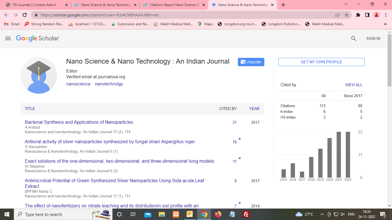
Google Scholar citation report
Citations : 142

Nano Science & Nano Technology: An Indian Journal received 142 citations as per Google Scholar report

Indexed In

  • CASS
  • Google Scholar
  • Open J Gate
  • China National Knowledge Infrastructure (CNKI)
  • Cosmos IF
  • Directory of Research Journal Indexing (DRJI)
  • MIAR
  • Secret Search Engine Labs
  • Universitat de Barcelona

View More

Recommended Conferences

Flyer