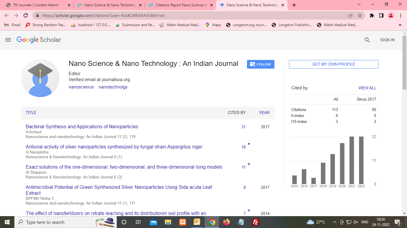
Current opinion
, Volume: 16( 4) DOI: 10.37532/ 0974-7494.2022.16(4).159Materials and Devices Using Nanotechnology in Electronics
- *Correspondence:
- Christopher Adams Editorial office, Nanoscience & nanotechnology: An Indian Journal, UK. E-mail:adams@nano.com
Citation: Adams C. Materials and Devices Using Nanotechnology in Electronics. Nano Tech Nano Sci Ind J. 2022; 16(4):159.
Abstract
The use of nanotechnology in electronic components is referred to as Nano electronics. These parts frequently have a size of just a few nanometres. Electronic components are, however, more difficult to produce the smaller they get. Nano electronics is the study of devices and materials that are so small that physical processes change the properties of the materials on a nanoscale. These devices rely heavily on interatomic interactions and quantum mechanical features to function.
Introduction
The use of nanotechnology in electronic components is referred to as Nano electronics. These parts frequently have a size of just a few nanometers. Electronic components are, however, more difficult to produce the smaller they get.
Nano electronics is the study of devices and materials that are so small that physical processes change the properties of the materials on a nanoscale. These devices rely heavily on interatomic interactions and quantum mechanical features to function. New phenomena prevail over those that rule the macro-world at the nanoscale. The features of these nanoscale devices are dominated by quantum processes like tunneling and atomistic disorder. Recent silicon MOSFET (Metal-Oxide-Semiconductor Field-Effect Transistor, or MOS transistor technology generations are already within this regime, including 22 nanometers CMOS (complementary MOS) nodes and succeeding 14 nm, 10 nm, and 7 nm FinFET (fin field-effect transistor) generations. Nano electronic devices have critical dimensions with a size range between 1 nm and 100 nm. Because current candidates differ greatly from conventional transistors, Nano electronics is frequently regarded as a disruptive technology. Electronics can now be faster, smaller, and more portable thanks to nanotechnology. It helps minimize power consumption and the size of transistors used in integrated circuits, while also boosting the power of electronic devices and memory chip density
Nano electronic devices
Spintronic: Spintronic is the study of and application of electron spin, coupled with its magnetic moment and electric charge, in solid-state devices. Given the conceptually difficult quantum physics and chemistry that underlie the issue, some people think it is esoteric, but the same thing was formerly stated about what is now considered mainstream electronics. Spintronic is a growing area of applied science and engineering that is also a fascinating pure science in and of itself.
Optoelectronics
Optoelectronic devices, or electronic devices that generate, detect, and control light, exist in a variety of designs. Optical communications that are extremely energy-efficient (less heat generation and power consumption) are becoming more and more significant because they may be able to address one of the main issues of our information age: energy consumption.
Materials used in nanotechnology include carbon nanotubes, nanofibers, and especially graphene, which has tremendous potential for use in optoelectronic devices (see, for example, "Light-emitting nanofibers shine the way for optoelectronic textiles").
Atomic electronics
Research on single-molecule electronic devices is extensive. These plans would heavily rely on molecular self-assembly, engineering the gadget parts to put together a larger structure or possibly a whole system by themselves. The current FPGA technology may perhaps be totally replaced by this for reconfigurable computing.
Future atomic-scale electronic systems may be possible because to the technology known as molecular electronics. The theoretical chemist and IBM researcher presented a promising application of molecular electronics in their works from 1974 and 1988.Memory, logic, and amplification Molecules.
Numerous nanowire topologies, including carbon and other material nanotubes, metal atom chains, cumulene or polyyne carbon atom chains, and numerous polymers, including polythiophenes, have been investigated as potential linking materials for Nano electronic devices.
Flexible electronics that can be worn
The fast-expanding selection of smart watches, fitness bands, and other cutting-edge, next-generation health monitoring devices, like electronic stick-on tattoos, are proof that the age of wearable electronics has arrived. However, if recent research is to be believed, wearable electronics will soon go far beyond tiny electronic gadgets and flexible, wearable computers. In addition to being embedded in textile substrates, these devices may eventually be transformed into the fabric itself by an electronics device or system. A new generation of clothing with distributed sensors and electronic features will be able to be designed and produced thanks to electronic textiles (or "e-textiles").
Displays
The three main categories of display technologies include organic LEDs, electronic paper and other devices that show still images, and field emission displays. Read our dedicated section on nanotechnology in displays for more information.
Electro molecular chemistry
Molecular electronics is concerned with electronic processes that take place in molecular structures like those found in nature, such as photosynthesis and signal transduction, as opposed to Nano electronics, where devices are shrunk down to nanoscale levels.
With the goal of developing a fundamental understanding of how charges move across molecules, molecular electronics is driven by the idea that tiny, potent, and environmentally friendly computers will be possible thanks to molecular circuits.
Benefits of Using Nanotechnology in Electronics Below are some benefits of Nano electronics
1. Increased memory chip density
2. The weight drops
3. Nanolithography is utilized in the manufacture of chips.
4. The size of transistors in integrated circuits decreases or is
5. Enhanced display displays for electronic gadgets
6. Lower power consumption