Original Article
, Volume: 12( 1)Electrical, Structural and Optical Properties of Cu3SbSe4 with High Thermoelectric Performance.
- *Correspondence:
- Batol Dabaa, Department of Physics, University of Aleppo, Aleppo, Syria, E-mail: batol.da@gmail.com
Received: Mar 26 2018; Accepted: May 29, 2018; Published: June 3, 2018
Citation: Dabaa B. Electrical, Structural and Optical Properties of Cu3SbSe4 with high thermoelectric performance. Nano Sci Nano Technol. 2018;12(1):124
Abstract
Cu3SbSe4 is a promising thermoelectric material due to high thermo power. Although it has a simple crystal structure derived from zinc blende structure. The thermoelectric properties of bulk of this semiconductor compounds, prepared by rapid hot press (RHP) technique at 270˚C while Cu3SbSe4 thin films were deposited onto glass substrate (microscopic slices) by chemical bath deposition (C.B.D) at (150˚C). Structure characterization was carried out using X-Ray Diffraction spectrum, in order to determine the average crystallite size which found in the range (20-30 nm). The obtained Cu3SbSe4 had p-type semiconductor has low resistivity in the range (0.124 Ωm). AFM micrographs of surface of the prepared film are observed that distance in the range (16-65) nm. The carrier density and Hall mobility in Cu3SbSe4 bulk were in the range 0.591×10¹⁸ Cm-3 and 117.3 Cm2/Vs. The band gaps of the Cu3SbSe4 film are determined from UV-Vis spectrophotometer are found to be within the range (1.25-1.5) eV while the energy band gap of Cu3SbSe4 bulk which determined from FT-IR spectrophotometer is (0.362eV) and it corresponds to wavelength (3417 nm). The power factor (PF) of Cu3SbSe4 samples is remarkably improved due to the optimization of whole concentration. Lattice thermal conductivity kL is very low which can be attributed to
Keywords
Electrical properties; thermal conductivity; XRD; RHP
Introduction
Synthesis of stoichiometric ternary metal chalcogenides by a simple approach is an attractive and challenging task due to their unique physical and chemical properties [1]. Since the last four decades, scientists have been attempting to find out alternative renewable energy sources to traditional energy sources. In recent years more efforts have been made to utilize the waste environmental energy by introducing alternative energy conversion routes such as solar cells [2], fuel cells [3], water splitting for hydrogen production [4], nanogenerators [5], as well as thermoelectricity. In the past few years copper containing chalcogenides have become promising materials due to their potential applications in photovoltaic, photocatalytic and thermoelectric devices. Now-a-days semiconducting materials of I–V–VI group chalcogenides gained increasing attention as they showed good electronic transport properties like low thermal conductivity, near-optimum band gap energy and a large absorption coefficient (>104 cm-1)[6]. Among the group I–V–VI elements Cu–Sb–Se forming highly conducting solid solutions with varying compositions such as Cu3SbSe3 and Cu3SbSe4 has been reported. With respect to its availability and low cost it was suggested as an alternative to CIGS [6].
Cu–Sb–Se has been studied as a promising material for photovoltaics as well as thermoelectric purposes. The thermoelectric materials are used to convert heat energy to electrical energy and their efficiency depends on the dimensionless figure of merit (ZT). The efficiency of a TE material is generally characterized by the dimensionless figure of merit ZT, defined as:
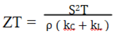 (1)
(1)
Where ρ, S, kC, kL and T are the electrical resistivity, Seebeck coefficient, thermal conductivity from carrier contribution, lattice thermal conductivity and absolute temperature respectively [7].
This thermoelectric material should have high electrical conductivity, high power factor (S2σ) and low thermal conductivity.
In these work Samples of bulk of Cu3SbSe4 was prepared using Rapid Hot Press (RHP) system and Cu3SbSe4 film was prepared using chemical bath deposition (CBD) system. structural properties of Cu3SbSe4 been studied by X-ray diffraction (X.R.D), AFM, absorption spectrum and IR spectrum , DC, Hal effects, Seebeck effects, Power factor, thermal conductivity, ZT and electrical resistivity measurements were carried out .
Experimental
Chemicals
EDA (99.7%), CuCl (97%), SbCl3 (99%) and selenium powder (99.0%).
Substrates cleaning
The cleaning of the substrate surface is significant for the characteristic of the film structure Cu3SbSe4 thin films were deposited on glass substrates by CBD method. Glass substrates were cleaned using an oxidant mixture (K2Cr2O7:H2SO4 - 1:10, HNO3, 1% EDTA) then rinsed with distilled water before deposition [8].
Cu3SbSe4 preparation
For preparation of Cu3SbSe4 2 mmol (SbCl3), 8 mmol Se and 40 mL (EDA) were put into a 100 mL glass beaker. After mixing uniformly, 60 mmol CuCl was then put into the same beaker. The solution was stirred by a magnetic stirrer at the speed of 1700 r s−1 maintaining a temperature of 150°C during the synthesis. Two glass substrates were introduced vertically in the chemical bath with the help of a suitably designed substrate holder. After films deposition, substrates were taken out and dried at 373 K for 30 minutes and kept at room temperature for further measurement after about two hours, a large quantity of powders was precipitated. Then the precipitates were collected, filtered and washed with anhydrous ethanol and distilled water until a pH value close to 7 was obtained, and then dried under vacuum at 60°C for nearly 6 h . The formed powder was grinded by a ceramic mortar, pressed under 10 ton/cm2 as disks of (3.11) mm diameter and 3.5 mm thickness. Then Cu3SbSe4 material pressed at (280°C) for (30 min) with rapid hot press system (RHP) are shown to agree with material consolidated under typical consolidation parameters. A rapid hot press system in which the heat is supplied by RF induction to rapidly consolidate thermoelectric materials is described. Use of RF induction heating enables rapid heating and consolidation of powdered materials over a wide temperature range (100-3700) °C. Such rapid consolidation in nanomaterial is typically performed by spark plasma sintering (SPS) which can be much more expensive. We have designed and fabricated a rapid hot pressing technique based on induction heating that is as fast, if not faster, than SPS for the rapid consolidation of materials without the effects of a dc current. Such a system will be ideal for maintaining small and nanometer scale microstructures. The technique is demonstrated by consolidating dense Cu3SbSe4 based thermoelectric materials at 553 K for 30 min. Fabrication and maintenance of this system will cost significantly less than commercial resistance heated or spark plasma sintering presses. The RHP system is an economic and robust system for research, development, and production of materials for a variety of purposes. Structural characteristics and morphology of the bulk materials were determined by X-ray diffraction (XRD) method using Philips X-pert Pro diffractometer at room temperature with CuKα radiation (λ=1.54 Å).
Results and Discussion
Structural studies
The XRD patterns of the samples of Cu3SbSe4 at room temperature are shown in FIG. 1. The powder XRD pattern seen in FIG. 1(a), that we do not observe any beak before (RHP). While after (RHP) in FIG. (1b). The main diffraction peaks correspond well to the standard JCPDS card (no. 01-085-0003) of Cu3SbSe4 with tetragonal structure. The lattice constant calculated was found to be (a = 5.655Å) for (112) plane. In FIG. (1c) we observe increase beak intensity with increasing RHP temperature.

FIG. 1. Shows the XRD profile of all the samples Cu3SbSe4.
a (Before (RHP)) , b (After(RHP) at (280°C) ) ,c (After(RHP) (350°C))
 (2)
(2)
 (3) (Bragg’s Law) [9]
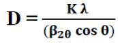
The crystallite sizes of Cu3SbSe4 are estimated by using Scherrer's formula [9,10]:
 (4)
(4)
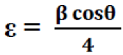
Where, K = 0.94 and λ is the wavelength of X-ray used which is Cu Kα radiation (λ = 1.54Å) and β2θ is the full width at half maximum (FWHM) of the diffraction peak corresponding to a particular crystal plane. The value of the crystallite sizes D (TABLE 1) varies within the range 20 to30 nm. The strain (ε) was calculated by the Formula 11:
| Cu3SbSe4 | (hkl) | a(Å) | d (Å) | D (nm) |
|---|---|---|---|---|
| Before (RHP) | (112) | 5.69 | 2.44 | 20 |
| After(RHP) | (112) | 5.66 | 2.31 | 30 |
| Strain ( ε × 10-4)(lines-2 m-4 ) | Dislocation Density (δ×1013) ( lines/m2) | |
|---|---|---|
| 54 | 25 | |
| 37 | 11 | |
TABLE 1. Structural parameters of Cu3SbSe4 bulk at room temperature.
 (5)
(5)
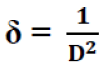
The dislocation density (δ), defined as the length of dislocation lines per unit volume of the crystal, was evaluated from the formula [11]:
 (6)
(6)
The result reveals that lattice parameters (a, d) decrease monotonically with increasing (RHP) temperature, as shown in TABLE 1.
Analysis of atomic force of Cu3SbSe4 (AFM)
FIG 2. AFM image of surface deposited film of Cu3SbSe4. We note that the structure in the form of granules with different sizes and measurements, where Horizontal distance in the range (16-65) nm.

FIG. 2. Shows AFM image of surface of the film of Cu3SbSe4.
It can be observed that the surface of the film is not very compact. Small crystallites or grains compose them. Round shaped clusters packed together constitute the film. We note many empty spaces can be seen between these clusters. The size of these small crystallites cannot be determined from these pictures. The average grain size is about 52 nm.
Optical studies
FT- IR spectral: FT-IR transition Intensity carried out in the range of wavelengths (2500- 25000 nm). FIG. 3 Shows the FT-IR transmission in function of wavelength, it indicate the energy band gab is (0.362eV) which corresponds to wavelength (3417 nm). FT-IR revealed the existence of some toxicity in the prepared samples before (RHP) but this toxicity reduces acutely after (RHP).

FIG. 3. IR transmission of Cu3SbSe4 in the wavelength range (2500-25000).
UV-Visible spectrum: The optical absorption of Cu3SbSe4 thin film was studied in the wave-length range 295 to 1100 nm. As shown in FIG. 4. Cu3SbSe4 film shows higher absorption at shorter wavelength side.

FIG. 4. Absorption spectra of Cu3SbSe4 thin film.
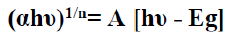
Energy band gab can be calculated using this formula 12.
 (7)
(7)
Where A is a constant, Eg is the band gap of the film. The exponent n depends on transition type. The values of n for direct allowed, indirect allowed, and direct forbidden transmissions are n = 1/2, 2, and 3/2, respectively. The intercepts of the extrapolated straight line at the (αhυ)n = o axis give the value of the Eg. The direct band gaps were obtained from the linear portion of (αhυ)2 vs. hυ plot as shown in FIG. 5(a), Its value is (1.25 eV). While the direct forbidden transition were obtained from the (αhυ)3/2 vs. hυ plot as shown in FIG. 5(b). Its value is (1.5 eV). The indirect band gaps were obtained from the (αhυ)1/2 vs. hυ plot and it doesn't exist.

FIG. 5. (αhυ) in function of hυ where:
(a) (αhυ)2 in function of hυ , (b) (αhυ)3/2 in function of hυ .
Electrical Measurements
Electrical resistivity measurement: The thermoelectric properties of Cu3SbSe4 are shown in FIG. 6. it clear that electrical resistivity ρ of Cu3SbSe4 decreases with increasing of temperature in the whole temperature range.

FIG. 6. Shows the temperature dependences of electrical resistivity for Cu3Sb1-xAlxSe4 (x = 0, 0.03, 0.05, 0.07).
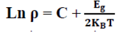
Determine the activation energy of Cu3SbSe4: In order to examine the temperature behavior of the resistivity for Cu3SbSe4, logarithm of the resistivity ρ as a function of reciprocal of temperature is given in the in FIG. 6. It can be seen that good linear relationships between Ln ρ and 1/T exist in the high temperature range for Cu3SbSe4. The existence of a linear relationship between ln ρ and 1/T means that the resistivity can be described by using a thermally activated expression in corresponding temperature regimes, written as:
 (8)
(8)
Where, C is consistent and kB Boltzmann constant (8.62 × 10⁻⁵ eV/K), E.g. band gap. By best fitting of experimental data in the above formula, TABLE 2 shows the variation of activation energy with (RHP), we note that the conductivity of the samples increases with (RHP).
| Sample | Ea (eV) |
|---|---|
| Before (RHP) | 0.25 |
| After (RHP) | 0.2 |
TABLE 2. Shows variation activation energy with (RHP).
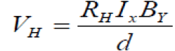
Hall effect measurement: The variation of Hall voltage (VH) with the current for Cu3SbSe4 at room temperature shown in FIG. 7. The lattice structure may be unstochiometric, and the interstitials control the conductivity type [12,13]. So that the prepared Cu3SbSe4 are p-type (Because of the Hall coefficient resulted is a positive signal).

FIG. 7. The variation of Hall voltage (VH) with the current for Cu3SbSe4.
 (9)
(9)
Due to the vacancies of sulfide ion [14,15] that means the conduction is dominated by holes [16].
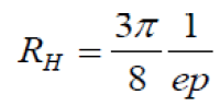
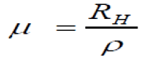
TABLE 3 show values of resulting parameters from Hall Effect studies. It was found that the carriers’ concentration and Hall mobility increase with (RHP) [14], where carriers’ concentration P, Resistivity ρ and Hall mobility μ are calculated.
| Sample (x) | (Before RHP) | (After RHP) |
|---|---|---|
| Hall coefficient RH×10-6(m3/C) | 2.08 | 1.05 |
| Carrier density PH×1018 (Cm-3) | 2.82 | 5.91 |
| Resisitivity ρ ×10-7 | 1.56 | 0.16 |
| Hall mobility μ × 10-2 (m2/V s ) | 177 | 133 |
TABLE. 3. Value of resulting parameters from Hall Effect studies.
According to the relationships [14]:
 (10)
(10)
 (11)
(11)
 (12)
(12)
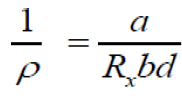
Where, a, b and d are the dimensions of the Cu3SbSe4 sample and RH is the hall coefficient.
The sample is p-type semiconductors, as verified by the positive Seebeck coefficients, which are shown in FIG. 8. The Seebeck coefficient S for Cu3SbSe4 increases with the increasing temperature. This is the typically characteristic of a heavily degenerate semiconductor.

FIG. 8. shows the Temperature dependences of Seebeck coefficient for Cu3SbSe4
The temperature dependences of power factor of Cu3SbSe4 are shown in FIG. 9. The PF of Cu3SbSe4 increases linearly with temperature. The temperature dependences of the lattice thermal conductivity (kL) for Cu3SbSe4 compounds in FIG. 10, k decreases with increasing temperature in the whole temperature range.

FIG. 9. shows the Temperature dependences of power factor for Cu3SbSe4.

FIG. 10. shows the Temperature dependences of the lattice thermal conductivity kL for Cu3SbSe4.
Lattice thermal conductivity kL is estimated by subtracting the carrier thermal conductivity kc from k where the Wiedemann–Franz relation with a Lorentz constant L0 is, applied for estimating kc
(kc = L0T/ρ) (13)
Here, L0 is set to (2 × 10⁻⁸ V2 K2) [16-18].
FIG. 11 shows the temperature dependence of ZT for Cu3SbSe4. The value of ZT reaches 0.35 for Cu3SbSe4 at 490 K. The elevation of ZT for Cu3SbSe4 results mainly from both its enhanced PF due to the optimization of hole concentration and reduced kL.

FIG. 11. Shows Temperature dependence of ZT for Cu3SbSe4
Conclusion
In summary, P-type Cu3SbSe4 crystals were fabricated through Rapid hot press system (R.H.P) technique. The electrical, structural and optical properties of Cu3SbSe4 properties were investigated. AFM micro-graphs of surface of the prepared film are observed that distance in the range (16-65) nm. Structure measurement determine the average crystallite size which found in the range (20-30 nm). The results showed that decrease in thermal conductivity, which can be attributed to the strong phonons scattering by atom mass fluctuations. The large drop of the resistivity is caused by increase in whole concentration. A large thermoelectric figure of merit ZT = 0.35 is obtained for Cu3SbSe4 at 490K.
References
- Aldakov D, Lefrançois A, Reiss P. Ternary and quaternary metal chalcogenide nanocrystals: synthesis, properties and applications. J Mater Chem C. 2013;1:3756-76.
- Beach JD, McCandless B E. Optical properties of CdSe and CdO thin films electrochemically. Thin Solid Films. 2007;32:225.
- Wang CY. Metal Organic Frameworks Route to in Situ Insertion of Multiwalled Carbon Nanotubes in Co3O4 Polyhedra as Anode Materials for Lithium-Ion Batteries. Chem Rev. 2004;104:4727.
- Huang G, Zhang F, Du X, et al. Metal organic frameworks route to in situ insertion of multiwalled carbon nanotubes in Co3O4 polyhedra as anode materials for lithium-ion batteries. ACS nano. 2015;9:1592-9.
- Cottone F, Frizzell R, Goyal S, et al. Enhanced vibrational energy harvester based on velocity amplification. J Intell Mater Syst Struct. 2014;25:443-51.
- Li XY, Xin HX, Zhang J. Improvement of thermoelectric properties of Cu3SbSe4 compound by In doping. J Alloys Compd. 2013;561:105.
- Heremans JP, Jovovic V, Toberer ES, et al. Enhancement of thermoelectric efficiency in PbTe by distortion of the electronic density of states. Science. 2008;321:554-7.
- Choudhury N, Sharma BK. Structural characterization of nanocrystalline PbS thin films synthesized by CBD method. IJPAP. 2008;46:261-65.
- Li Y, Qin X, Li D, et al. Transport properties and enhanced thermoelectric performance of aluminum doped Cu3SbSe4. Rsc Advances. 2015;5:31399-403.
- Yang C, Huang F, Wu L, et al. Effect of Zn substitution at a Cu site on the transport behavior and thermoelectric properties in Cu3SbSe4. Phys. D: Appl Phys.2011;44, 295404.
- Bhatt N, Vaidya R, Patel SG, et al. X-ray diffraction studies of NbTe 2 single crystal. B MATER SCI. 2004;27:23-5.
- Pankove JI. Optical Processes in Semiconductors, Prentice-Hall Inc, Englewood Cliffs, 1971.
- Obida MZ, Afify HH, Abou-Helal MO, et al. Nanocrystalline anatase titania thin films synthesized by spray pyrolysis for gas detection. Egyptian J Solids. 2005;28:35-51.
- Salim SM, Hamid O. Growth and characterization of lead sulfide films deposited on glass substrates. RE. 2001;24:575-80.
- Stancu V, Buda M, Pintilie L, et al. Chemically prepared nanocrystalline Cu3SbSe4 thin films thin solid films. 2008; 516,4301-6.
- Ubale AU, Junghare AR, Wadibahasmi NA, et al. Some electrical properties of thin Cu3SbSe4 films. Turk J Phys. 2007;31:279-86.
- Salim SM, Hamid O. Growth and characterization of lead sulfide films deposited on glass substrates. RE. 2001;24:575-80.
- Stancu,V, Buda,M, Pintilie L, et al. Chemically prepared nanocrystalline PbS thin films. thin solid films. 2008;516:4301-6.